Multilayer circuit boards are rarely “right the first time.” As layer count increases, stack-up structure, material lot variation, fabrication tolerances, and end-use test conditions all introduce variables — so even a design that passes simulation cleanly can still show signal or reliability problems once it comes off the production line. Understanding the technical roots of these problems, and knowing which ones can be resolved through a targeted adjustment rather than a full redesign, is the real basis for evaluating the engineering capability of a multilayer PCB supplier.
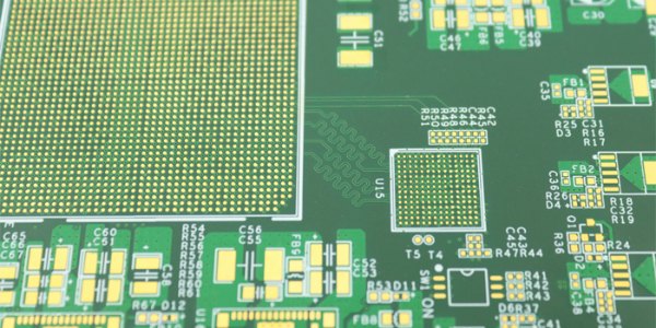
Building a multilayer board is closer to constructing a precise layered structure than printing a simple circuit: how each copper layer is routed, what insulating material separates the layers, and how stable that material’s thickness and dielectric properties are — together these form the “stack-up,” which directly determines whether the finished board meets its designed electrical performance. A capable supplier doesn’t wait until final test to get involved; it participates in manufacturability review from the design stage onward.
Design Errors Discovered During Validation
Stack-Up Structure and Simulation Deviation
Computer simulation is typically based on idealized material thickness and layer spacing, while actual lamination on the shop floor carries real tolerances — resin flow during prepreg (PP) lamination, copper thickness distribution, and interlayer alignment can all deviate slightly from the design values. For low-frequency circuits this deviation is usually negligible, but for high-speed signals it can translate directly into excessive crosstalk or timing that falls outside spec. An experienced supplier will run stack-up simulation software to calculate characteristic impedance during design file review, and flag risky via placements before production — for example, pointing out that a particular via layout will lower yield under the current process — rather than running the job as-is and dealing with scrap afterward.
Footprint and Via Alignment Deviation
The more layers a board has, the tighter the interlayer alignment tolerance needs to be. If a footprint in the schematic doesn’t exactly match the pin pitch of the component actually sourced, lamination can produce pad misalignment, delamination, or poor via fill. A mature supplier will cross-check Gerber files against the BOM before releasing to production, and apply extra alignment tolerance analysis to high-density BGA regions.
Raw Material Management and Supply Chain Response
Copper-clad laminate and prepreg pricing and lead times are heavily influenced by the global market, and certain imported substrates can become tight on supply during specific periods. A stable supplier typically maintains long-term relationships with multiple laminate manufacturers and keeps a list of backup materials with comparable performance from different sources (for example, comparing Tg170 substrates across vendors), allowing a quick source switch during a material shortage without disrupting the delivery schedule. This judgment can’t be made from a datasheet alone — it also requires weighing fundamentals like long-term material stability and the bond strength between copper foil and dielectric layers. These seemingly ordinary factors are exactly what determines whether a product keeps working reliably under harsh field conditions.
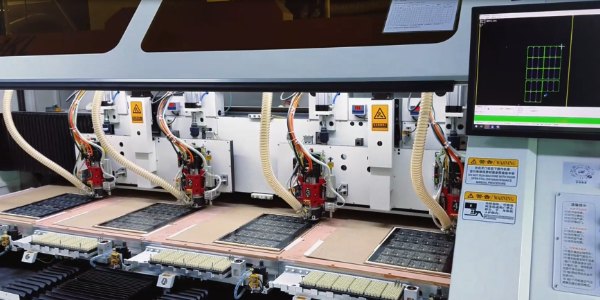
Volume Production Process Optimization
Thermal Management
Uneven resin flow during lamination can significantly reduce a board’s local thermal conductivity, causing the actual temperature rise distribution to diverge from what was designed. If measured temperatures exceed expectations, a supplier can improve thermal performance by increasing copper thickness, adding thermal via arrays, or optimizing copper pour on the power layers — usually without touching the overall design.
Signal Integrity Optimization
High-speed, high-frequency products are sensitive to crosstalk and return loss. A supplier can reduce signal attenuation by tightening etching precision, improving the integrity of the reference ground plane, and adjusting the spacing between traces and the ground plane. Where needed, re-sequencing the power and ground layers, or adding small filtering components, can stabilize communication lines — adjustments that typically don’t require redesigning the entire board.
Regulatory and Compliance Updates
Certification requirements vary significantly by industry: medical products typically need to meet IPC-6012 Class 3 and ISO 13485; automotive electronics often require IATF 16949 certification along with IPC-A-600 inspection standards; consumer products generally require UL94V-0 flame-retardancy certification plus RoHS and REACH compliance declarations. A qualified supplier should be able to provide complete third-party test reports and process records as objective evidence — not just verbal assurances.
Cost Reduction Opportunities
Without compromising performance, a supplier can help reduce cost along several dimensions: adjusting copper weight on non-critical layers from 2oz to 1oz, optimizing panel utilization to cut material waste, or substituting a domestically sourced substrate with equivalent performance where allowed. These adjustments should go through joint review between the supplier’s engineering team and the customer to confirm there’s no impact on electrical performance or long-term reliability before implementation.
Prototype Iteration and Product Evolution
Products going from prototype to volume production typically go through multiple rounds of design iteration. An experienced supplier builds in some process flexibility during small-batch pilot runs — for example, reserving test points or spare vias/connectors — so that when a design needs a minor tweak, it can be validated through jumper wiring or localized rework rather than restarting the entire process each time. This approach breaks what could be one disruptive major change into a series of controlled, incremental adjustments, shortening the iteration cycle.
Quality Control and Failure Analysis
Case study: Diagnosing intermittent failures in a 12-layer industrial control board during environmental testing.A project using a 12-layer board experienced roughly 3% of boards failing with inner-layer opens during high-temperature aging tests, in a recurring pattern across batches. Rather than pointing to a design flaw, the supplier’s engineering team ran cross-section analysis, sectioning the failed boards layer by layer and measuring layer thickness and copper plating under a microscope against the design requirements. The root cause was traced to uneven copper plating thickness at specific inner-layer vias — uneven current distribution across the plating rack in high-density via regions, compounded by plating process parameter drift in that particular batch, resulted in localized thin plating. The supplier then adjusted the plating parameters and rack layout, and applied targeted screening and rework to work-in-process boards rather than scrapping the entire batch outright. The aging test pass rate on subsequent batches recovered to above 99.6%.
This case illustrates why a supplier’s quality traceability system matters. A well-built traceability system shouldn’t stop at a final inspection report — it should be able to provide cross-section photos and plating process parameter records, and tie that data back to a specific batch or even an individual board, down to the responsible workstation or piece of equipment if needed. This depth of record-keeping — not just having advanced equipment — is what actually indicates genuine failure-analysis capability.
Balancing Risk and Practicality
The choice between rework and redesign requires weighing cost, time, safety, and long-term maintainability. Where structural flaws are widespread, especially involving safety-critical functions, redesign is usually the safer path. Where an issue is localized and its root cause can be pinpointed, targeted process adjustment is generally the more practical option. Every change should be fully documented to support future traceability and servicing. When evaluating a supplier’s design-for-manufacturability (DFM) capability, it’s worth focusing on:
- Whether they proactively raise stack-up and process feasibility feedback during design review
- Whether they have real failure-analysis and batch-traceability capability (cross-section records, process parameter records)
- Whether they maintain a stable raw material supply base with viable backup sources
- Whether they build in process flexibility between prototyping and volume production (test points, spare vias, etc.)
- Whether they can back claims with third-party certifications and test reports
Modern electronics depend heavily on multilayer circuit boards, and the industry itself keeps moving fast — materials, processes, and end-application requirements are all continuously evolving. Flexibility and traceability are the core capabilities needed to keep up with that change. The value of an engineering-capable multilayer PCB supplier isn’t reflected in a quote sheet or an equipment list — it shows up in whether they can prevent problems through systematic design review before they happen, and, when problems do occur, resolve them with solid failure-analysis skills that minimize the damage. This kind of disciplined, forward-looking process management is what ultimately allows a manufacturer to respond quickly when reality doesn’t match expectations.