Also known as silicon-based OLED or OLEDoS, Micro-OLED differs from conventional AMOLED with external driver ICs. While large-scale display applications rely on direct-view technologies like a modular led wall—frequently deployed through the commercial led wall rental market for events, staging, and virtual production—Micro-OLED leverages advanced CMOS semiconductor manufacturing to integrate driver circuits directly onto a single-crystal silicon wafer. This compresses pixel size to one-tenth that of traditional displays, achieving ultra-high pixel density (PPI) micro-displays [1].
On the end-market side, Apple Vision Pro has spurred iterations of high-end XR headsets, making silicon-based OLED an increasingly dominant option for premium VR hardware. In consumer AR, silicon-based OLED paired with Birdbath optics has become a proven, mature solution for consumer-grade AR glasses.
- Micro-OLED Device Structure and Manufacturing Workflow
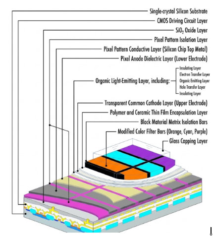
As a subset of organic light-emitting-diode technologies, Micro-OLED uses monocrystalline silicon wafers as its substrate. Compared with glass-based OLED, silicon delivers higher carrier mobility and supports tiny pixel cells ranging from 6 μm to 15 μm. The device consists of two core building blocks: the silicon-based driver backplane and the OLED light-emitting front-end.
1.1 Two Core Device Building Blocks
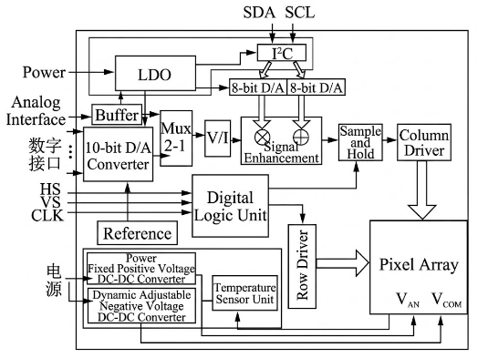
► Silicon-based Driver Backplane Through CMOS processing, Micro-OLED integrates timing-control modules, row-column scan drivers, power-management units and TFT pixel-switch arrays inside a monocrystalline-silicon die. This eliminates numerous external wiring traces, enables miniaturisation and lightweight design, and reduces signal-path losses.
► OLED Light-Emitting Front-End The light-emitting stack comprises an anode, multi-layer organic functional films, a cathode and a colour-filter layer. The anode-cathode stack forms the power supply loop. Organic functional layers include a hole-injection layer, hole-transport layer, emissive layer, electron-transport layer and electron-injection layer. Under an applied electric field, holes and electrons migrate toward each other and recombine to form excitons. Excitons relax and emit photons to produce light. The colour-filter layer decomposes white light into red, green and blue primary colours, whose mixing generates full-colour imagery.
1.2 Five-Step Micro-OLED Manufacturing Workflow
Silicon-based Backplane Fabrication IC-design houses develop digital-logic chip designs, while panel suppliers define pixel-array circuitry. The combined layouts are sent to silicon foundries for CMOS tape-out and wafer fabrication, producing finished silicon backplane wafers with fully integrated pixel circuits.
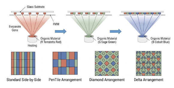
Organic-Emitter Evaporation Metal anodes are deposited atop silicon wafers. Under high-vacuum conditions, the hole-injection / transport layers, emissive layer and electron-transport / injection layers are sequentially evaporated. A transparent cathode is deposited last to complete the light-emitting-stack deposition.
Thin-Film Encapsulation PECVD and ALD systems alternately deposit hybrid inorganic-organic encapsulation films. These barrier layers block moisture and oxygen to suppress degradation of organic emissive materials. Inorganic layers provide primary water-oxygen barrier performance, whereas organic layers act as stress buffers to mitigate delamination and cracking induced by thermal expansion and contraction.
Colour-Filter Fabrication and Cover-Glass Bonding Photolithography, photoresist coating, exposure and development are used to pattern RGB colour filters and black-matrix structures for pixel-level colour isolation. The colour-filter cover glass is bonded to the device with UV-cure adhesive to form a protective cavity.
Back-End Module Processing Wafers are diced into individual display dies. After optoelectronic performance screening, known-good dies are bonded to PCBs, protected by dispensed encapsulant glue, and subjected to burn-in screening to produce finished display modules.
Micro-OLED Full-Industrial-Chain Breakdown
The OLEDoS ecosystem represents a characteristic cross-domain fusion of semiconductor and display industries. Upstream segments cover silicon wafers, fine-chemical materials, semiconductor / evaporation equipment, inspection tools, chip design and silicon foundry services. Mid-stream activities focus on Micro-OLED panel manufacturing. Down-stream participants include system integrators and solution providers serving XR, industrial and medical applications.
► Silicon-Based Backplane Segment Panel vendors and chip-design firms jointly define pixel-circuit and driver-logic specifications, which are then realised via CMOS wafer fabrication at foundries. Several companies possess end-to-end capabilities spanning chip design, device R&D and panel production. Foundry process capability directly governs backplane integration density and achievable yield.
► Key Upstream Raw Materials The bill-of-materials includes silicon substrate wafers, anode metals, complete sets of organic emissive materials, organic / inorganic encapsulation films, photoresists, developers, strippers, colour-filter photoresists and black-matrix materials. Organic emissive materials constitute a major performance bottleneck. Constrained by fine-chemical barriers, high-grade material supply is concentrated among Japanese, South-Korean and European-American suppliers.
► Core Manufacturing Equipment Critical hardware includes high-vacuum evaporators, lithography tools, etchers and ALD / PECVD thin-film-deposition systems. The evaporation-equipment market is oligopolistic: Japan’s Canon Tokki holds a long-standing dominant position. South-Korea’s Sunic System has drawn industry attention by launching RGB-independent evaporation equipment optimised for Micro-OLED. Domestic suppliers are also advancing the localisation of high-precision evaporation systems.
► Inspection Equipment Inspection tools run throughout the manufacturing workflow, performing optical, electrical, signal and defect metrology to reject faulty dies and boost final yield. Given OLEDoS’s far higher resolution and refresh rate compared with conventional displays, inspection hardware demands superior resolution, sampling speed and integration. Inspection-equipment vendors are therefore expanding offerings into mid-to-late-stage silicon-wafer test workflows.
► Mid-Stream Panel Manufacturing European, American, Japanese and South-Korean players entered the Micro-OLED market early and accumulated substantial proprietary know-how. Representative firms include eMagin (US), Sony (Japan), Microoled (France), Fraunhofer (Germany) and LG Display (South-Korea). Driven by rising XR-market momentum, domestic enterprises are accelerating R&D and mass-production efforts for consumer-grade silicon-based OLED panels.
► Down-Stream Application Scenarios Target use-cases centre on near-eye-display hardware: VR/MR headsets and AR glasses, alongside electronic viewfinders. Additional professional-domain applications cover automotive HUDs, industrial inspection equipment, high-end medical devices and night-vision systems. At present, industrial resources and capital attention are heavily focused on consumer-oriented AR/VR markets.
Gradual resolution of mass-production bottlenecks has driven price reductions for AR glasses, making such hardware accessible to mainstream consumers. This market shift has fostered a growing ecosystem of dedicated Micro-OLED solution providers and manufacturers. One notable player is Shenzhen Pengsheng MicroVision Tech from Shenzhen, China, recognised for delivering turn-key solutions for downstream customers.
References
1.Zhan, T., Yin, K., Xiong, J., He, Z., & Wu, S. T. (2020). Augmented reality and virtual reality displays: emerging technologies and future perspectives. iScience, 23(8), 101397.
2.Ghosh, A., Khayrullin, I., Chu, T., et al. (2005). High-brightness active-matrix OLED microdisplays. Journal of the Society for Information Display, 13(7), 567-573.
3.Vogel, U., Kreye, D., Richter, L., et al. (2010). OLED-on-silicon microdisplays: technology and applications. Proceedings of SPIE, Vol. 7722, 77220B.
4.Motoyama, Y., Matsui, K., Yamashita, K., et al. (2017). A 0.23-inch FHD OLED Microdisplay on Silicon Backplane. SID Symposium Digest of Technical Papers, 48(1), 1362-1365.
5.Choi, S., Kim, J., & Lee, H. (2021). Ultra-high-resolution OLED microdisplays based on white OLED with color filters. IEEE Transactions on Electron Devices, 68(10), 5012-5018.
6.Shenzhen Pengsheng MicroVision Tech Co., Ltd. (2026). How AR/VR OEMs Can Efficiently Integrate Microdisplay Solutions and Supply Chains.
7.Ali, M. U., Miao, J. S., Rhee, S. J., et al. (2023). Micro-OLED technology for near-eye displays: A review. Journal of Information Display, 24(2), 85-102.
- Shenzhen Pengsheng MicroVision Tech Co., Ltd. (2026). LCoS, Micro-OLED on Silicon, MicroLED, and LBS: A Comparative Analysis of Four Near-Eye Display (NED) Technologies.
- MediA Flow Studio (2025). 4K TV vs. LED Wall Rental: A Comparison for Conference Display Solutions