The modern industrial landscape demands smaller, more efficient, and highly durable components. Meeting these rigorous standards requires manufacturing processes with precision scaled down to the atomic level. Sputtering targets serve as essential source materials utilized in thin-film deposition environments to create highly precise microscopic coatings. Today, these materials are widely used across electronics, optics, solar technology, semiconductors, displays, medical devices, biocompatible coatings, and advanced manufacturing. As industries demand components that perform reliably under heat, wear, corrosion, and other stress conditions, sputtering targets have become essential for producing high-performance thin films.
What Are Sputtering Targets?
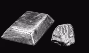
Sputtering targets are specialized solid materials utilized inside physical vapor deposition (PVD) or sputtering systems. During the standard sputtering process, localized atoms are systematically ejected from the target and deposited tightly onto a substrate, ultimately forming a functional thin film. The target acts as the primary source material, and the deposited film often closely reflects the target material’s composition, although final film properties can vary depending on process conditions, substrate type, and whether reactive sputtering is used. These functional source materials may be precisely manufactured from solid metals, complex alloys, advanced ceramics, structured oxides, solid nitrides, or robust composite materials. Engineers use sputtering when they need controlled film thickness, uniform coatings, and reliable material performance.
How the Sputtering Process Works
The sputtering process proceeds through these essential operational steps:
-
The target and substrate are placed inside a sealed vacuum chamber.
-
An inert gas, typically high-grade argon, is purposely introduced into the chamber.
-
The system generates high-energy electrical plasma inside the contained chamber.
-
Accelerated plasma ions strike the surface of the dedicated sputtering target.
-
This kinetic energy forcefully knocks atoms loose from the target material.
-
The released atoms travel across the chamber and deposit onto the substrate as a thin film.
This precise deposition method brings significant value to production environments. It helps create uniform barrier coatings and allows for precise film thickness control. It actively manages countless distinct solid material types seamlessly and functions correctly across both delicate isolated target research initiatives and massive industrial-scale manufacturing deployments.
Common Sputtering Target Materials and Their Uses
Selecting the right material depends on the properties required in the final thin film. Deposition engineers evaluate necessary baseline electrical conductivity, targeted optical reflectivity, required physical hardness, external transparency, heavy chemical corrosion resistance, and specific functional thermal stability to define the final target structure.
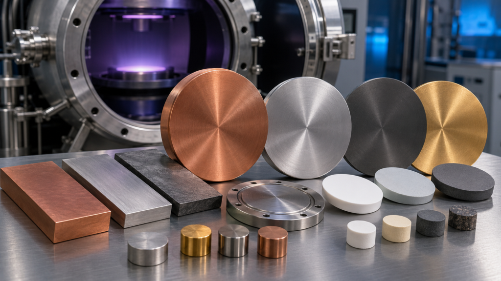
Metal Sputtering Targets
Mass manufacturing relies heavily on pure metallic elements like solid aluminum, conductive copper, protective titanium, gold, hard chromium, stable nickel, and native silver to form foundational layers. Metal sputtering targets are commonly selected when the finished thin film needs conductivity, reflectivity, adhesion, or barrier performance. For example, copper and aluminum are often used for conductive layers, titanium may support adhesion or barrier functions, and a silver sputtering target may be selected for reflective or highly conductive thin films.
Alloy Sputtering Targets
Alloy targets combine two or more metals to create film properties that single-element targets may not provide. Engineers deliberately deploy mixed alloys when the manufacturing framework explicitly necessitates notably superior base surface hardness, heightened comprehensive corrosion resistance, fine-tuned electrical parameter behavior, or profound structural thermal stability across massive temperature shifts. Core operational deployments regularly feature standard nickel-chromium frameworks, high-stress titanium-aluminum pairings, varied complex copper alloys, and proprietary custom alloy configurations.
Ceramic and Compound Sputtering Targets
Technical facility executives leverage complex non-metallic ceramic and mixed compound sputtering targets whenever the manufactured structural surface demands specific visual optics, heavy electrical layer insulation, precise environmental transparency, or rugged physical protective traits. Highly widespread applications incorporate compounds explicitly featuring electrically insulative silicon dioxide, visually refractive titanium dioxide, and specialized conductive zinc oxide models. Furthermore, highly standard indium tin oxide maintains widespread dominance across transparent applications, while heavy aluminum oxides, fundamental structural dense nitrides, and highly stable solid carbides successfully shield volatile operational endpoints.
Key Industrial Applications of Sputtering Targets
Sputtering targets are uniquely utilized cross-industry wherever exact surface properties matter precisely as much as the fundamental structural base material underneath.
Semiconductors and Microelectronics
The modern semiconductor industry depends absolutely on highly controlled deposition because even microscopic film defects can severely damage overall electronic component performance. Manufacturers regularly deploy specific conductive layers, protective barrier layers, precise seed layers, and conductive electrical contacts. This tight precision consistently guarantees the structural thin-film layers desperately required for manufacturing incredibly complex microchips, intricate integrated circuits, and precision electronic devices.
Optical Coatings and Displays
Optical applications explicitly require advanced coatings carefully finalized with strict material transparency, targeted physical reflectivity, and long-term durability. By utilizing exact sputtering targets, mass manufacturers generate vital highly reflective coatings and critical anti-reflective coatings. These components successfully build modern capacitive touchscreens, ubiquitous commercial LCD and OLED displays, sophisticated precision optical filters, and specialized architectural mirrors alongside industrial lenses.
Solar and Energy Technology
Sputtering helps create consistent films across large surfaces, which makes it useful in solar panels and related energy applications, functioning as incredibly valuable performance metrics within massive solar panel systems and related energy manufacturing. System protocols mandate generating highly standard thin-film solar cells, heavily specialized transparent conductive layers, structural rear back contacts, critical reflective layers, and widespread energy-efficient coatings intended for heavy-duty modern infrastructure.
Medical, Aerospace, and Protective Coatings
Industrial sputtering actively improves robust external surface performance entirely without chemically or mechanically changing the base material itself. These precise processes apply heavy functional wear-resistant coatings, strict protective corrosion-resistant coatings, and biocompatible surface coatings directly onto delicate sophisticated medical device coatings. They can also help protect high-stress aerospace components and industrial surfaces exposed to demanding operating conditions.
Why Purity, Density, and Consistency Matter
Buyers should strictly avoid evaluating and acquiring industrial sputtering targets based solely on matching material names. Instead, recognize that sputtering target quality comprehensively controls the final produced thin-film quality parameters. High-purity targets help reduce the risk of unwanted contamination during deposition. Dense targets help support stable performance across repeated production runs. Perfecting consistent microstructural composition actively safeguards necessary batch repeatability goals. Poor-quality targets can cause film defects, uneven coatings, arcing, and process instability. Consequently, rigorous precision sectors demanding tight control—expressly heavy semiconductors, precision optics, and medical technology—functionally demand considerably tighter active supplier quality control frameworks.
How to Choose the Right Sputtering Target
Securing the objectively optimal specific sputtering target demands carefully balancing detailed required properties defined by both the functional thin-film endpoint and the exact physical deposition rig configuration. Successful engineering and corporate procurement chains should exhaustively define all application demands beforehand, only then explicitly selecting optimal base material and precise geometric specifications. Exacting selection directly necessitates reviewing fundamental target chemical material composition, absolutely required trace purity minimums, distinct projected film functions, deep foundational substrate material compatibility guidelines, physical block sizing and customized dimension shaping requirements, explicit operating structural thickness configurations, and structural baseline backing plate bonding requirements. Procurement teams should also confirm whether the target will be used in DC sputtering, RF sputtering, or reactive sputtering, since each process can affect material choice and specifications. They should also define whether the target is for R&D or high-volume production and review supplier documentation for quality control.
Next Steps for Selecting Sputtering Targets
Executing a consistently high-quality functional physical vapor deposition process directly requires engineers to execute these definitive next steps:
-
Calculate and fully define exactly which explicit functional film properties the final component needs.
-
Accurately choose proper precise target materials logically mapped directly to strictly required framework conductivity, measured reflectivity, exact physical base hardness, optical structural transparency, or environmental corrosion resistance standards.
-
Validate detailed dimensional target geometry configurations, expected purity grade standards, calculated operating material density, and backing bonding compliance frameworks.
-
Heavily calibrate and formally sync the targeted component material against specific internal system limits and baseline production processing scale thresholds.
-
Partner deliberately with heavily validated, technologically rigorous suppliers that actively provide high-tier technical structural specifications alongside reliable continuous quality validation capabilities.
Ultimately, functional sputtering targets represent the functional heart of broad thin-film manufacturing. Choosing the right materials improves coating durability, supports process stability, and helps manufacturers produce more reliable products.