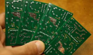
Printed Circuit boards are the basic building blocks of any electronic device. However, before you have a completed PCB, there are several manufacturing processes it has to undergo.
One primary PCB manufacturing process is PCB milling. PCB milling or isolation milling is a procedure that helps you to cut down the overall costs of a PCB. Below is everything you need to know about PCB milling.
What is PCB milling?
PCB milling or isolation milling is the process of scalping a section or sections of copper traces from a PCB. The scalped area offers enough space for the recreation of pads, various structures, and signal traces.
PCB milling and PCB etch are two similar subtractive processes with an aim of achieving the same results. However, PCB etching is a process that uses a chemical mixture.
With PCB milling, there are no chemicals. Hence, it is the perfect option for people without a lab environment for PCB etching. Keep in mind that etching chemicals are corrosive and produce unsafe fumes.
Although PCB milling is safer, the quality of the board depends on various factors. Some of these factors include milling accuracy, the control, and the trueness of the system. So, if the milling bits are tempered or incorrect, the results will not be desirable.
PCB Milling Process
PCB milling process comprises the hardware and software systems. The user interacts with the hardware system to create a prototype board through the software interface.
*Software system – You can use vector or raster software packages here. But you do not need to think much about the software packages and the device’s manufacturer supplies them.
*Hardware system – this is a numerically controlled machine. The system can have a parallel or serial port to connect to the main controller. There is movement along the X/Y axis that is facilitated by stepper motors. But on the Z-axis, it is powered by a non-monitored lead screw.
Type of Tools for Milling
Some popular PCB milling tools include V tools kit, drill tools, rubout tools kit, router bits tools, and many others.
Advantages of PCB milling
*PCB milling is great for PCB prototyping when making special PCB designs. This is because it does not fabricate the circuit board with chemicals.
Unlike PCB etching, where chemicals are used, it is possible to make your own PCB at home since milling does not require chemicals.
*Prototyping with a CNC machine helps you to eliminate the wet process. Unlike the wet process, where it is not easy to fabricate high-resolution boards, a CNC machine is helpful for milling, drilling, and cutting.
*Some boards offer a challenge when handling the wet process, and others can get damaged. Therefore, the best option to consider is PCB milling.
Tips for PCB milling
Many people try and fail during the PCB milling. To help you succeed in the process of PCB milling, here are a few tips you need to know.
1. Leveling
PCB milling is subtracting a thin layer of metal from the board. Hence, you need to ensure a uniform level. This can be achieved through physical leveling or computer leveling.
2. Track clearance
You need to pay attention to the mill’s clearance and adjust it accordingly. For instance, most users need a 0.05mm track clearance.
3. Gcode files
If the CNC machine can handle the three operations, cutting, drilling, and milling, ensure you have a gcode file for every procedure.
4. Coating
You need to coat the exposed copper. The best way to protect it is by applying a solder mask.
5. Safety
You need to ensure you observe the machine operation guidelines. This will ensure you are safe when using a PCB machine. However, there is dust that comes from drilling fiberglass.
To be safe, control the dust with a vacuum cleaner to avoid inhaling it. There are also softer and non-dusty copper clad boards that can solve the problem.
Essential things you need to know about PCB milling
*With a Software system, the PCB manufacturer offers the application needed for PCB milling.
*Since there is no use of chemicals, PCB can be done in a lab environment without dangerous chemicals.
*Although some factors affect PCB milling, the milling process can be through within 30 minutes.
*The accuracy and sharpness of the milling bits used can directly affect the quality of the board.
*The two main software packages used are Vector and Raster.
*Nevertheless, Vector depends on the data offered by Raster. On the other hand, Raster needs a less operating resolution.
PCB milling vs. Etching
Etching is a chemical process that demands film laser imaging. On the other hand, PCB milling does not need chemicals. Nevertheless, Etching may cost less.
Etching is a chemical-loaded process. Hence, it can only be administered in a factory setting. You can perform PCB milling in a lab even though no chemicals are involved.
Conclusion
PCB milling is a perfect and cost-effective method of creating solid and high-quality PCBs from existing ones. Hence, knowing the process and the essential tips can help you get started. The process is more straightforward, and you do not handle hazardous chemicals.