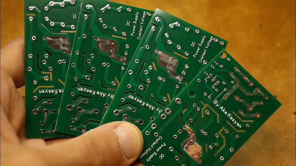
PCB clone, also named as PCB copy board or PCB reverse engineering, PCB clone refers to reverse engineering of PCB design. First, the PCB circuit board is removed and a BOM list is made of its components. An empty board/pic is scanned in and run through copy software to get it back to a pcb file. The pcb file is transferred to the PCB factory for production of a bare board, and then a queue for components ( According to the BOM order, the components are purchased one by one), and in exactly the same way as the original PCB circuit board. PCB copying technology can also be used to realize imitation of electronic products and electronic product cloning. The so-called board modification is the process of doing reverse technical research based on the design PCB board.
How to copy PCB board?
BOM production and disassembly
The first step in PCB board cloning is the generation of BOM list. This file is essential for the subsequent purchase of parts, all functional modules of the PCB board, and finally, the welding and debug of PCB clone board. This list is essential in board copying and design, as it contains the necessary parameters and specifications of all components on the PCB.
[BOM list must specify contents in BOM: component name, component specification, component position number, component material number, component material specification, shape and shape code of components, etc. BOM list preparation steps:
Preparation
The PCB is the main hardware of the board, and it will take two photos of the vitality components on it with a digital camera. Use paper to record the model, parameters and the locati0n of all vitality components above and down, particularly the direction of diode, triode and IC notch.
Dismantling records
Take each part out one at a time. In the process of dismantling the board, the intact original board is separated into bare boards and components. During the disassembly process, it is crucial to create a BOM list. Professional board dismantling personnel will prepare a piece of white paper and a pen before copying the board, and first write down the serial number, and the position number of the components on the paper. Put the position number corresponding to each component on white paper with double-sided tape after removing it. When splitting the board, it is worth mentioning that all component numbers need to be arranged with care, because if one component locati0n information is wrong, the entire BOM list will be wrong, affecting the cloning effect.
Component testing
This is where the board dismantling personnel obtain the sequence list recording component information, and they officially enter the BOM Production Process — a process of compiling through testing and analysis all parameters related to components into an information table.
Make a BOM list and check it
The FAB list is constructed from a table of diverse test data, part models, and attributes, as well as specificities.
Material procurement
Influence of BOM Production Efficiency on Later Production The BOM list is the main basis for rearranging components and the material basis for subsequent product production. So its production efficiency will be a key influence in later processes.
scanning
1) Scan each layer of the printing plate using a scanner and convert them to an image format acceptable to conversion software, such as BMPTOPCB and QUICKPCB. Video files. The image format is usually the BMP format,That is to say, the PCB must be placed horizontally and vertically into the scanner, otherwise PROTEL cannot synthesize the reverse image and the file surface cannot be saved.。 Steps: Take the tin out of the PAD hole. Wipe the PCB with alcohol, and then insert into the scanner. You need to increase the scanning pixels a bit to scan when the scanner scans so that it can obtain clearer images! You run POHTOSHOF, scan the silk screen surface (in color), save the file and Print it out to keep for later use. In order for the copper film to shine, please LIGHTLY POLISH ON THE TOP LAYER AND THE BOTTOM LAYE layers USING WATER GAUZE PAPER. Insert it in the scanner: Open PHOTOSHOP and scan the two layers as a color. In the fourth step, we adjust the contrast and lightness of the canvas so that copper film and non copper film have a strong difference. Then turn the image to black and white and see if the lines are sharp. If not, repeat this step. Save the image TOP in black and white (BMP) format files if clear. BMP and BOT. BMP. PHOTOSHO P You can use PHOTOSHO P to fix and correct graphic problems. Making two BMP format files into PROTEK format files, and transferring two layers by PROTEL. If the PAD and VIA positions after two layers are basically coincident, proving the front few steps do good. If the scan deviates then Repeat it again.
PROTEL synthesis
Open AUTO CAD software, prepare a new CAD file, in the Insert menu choose Insert bitmap image. After you choose the image that you wish to insert, a dialog box named the Insert Image box will show up. Choose a 1:1 ratio in the dialog box. Insert PCB image. Create a rectangular box that encapsulates the edge of the PCB diagram. agdNote: You should make use of the object defined tracking object lock point when rendering the border It is better to put a border in the circuit to avoid image moves by mistake during the drawing process, it becomes hard to register. up•
Draw the component footprint. The component package used on the PCB board that needs to be replicated does not have to be the same as the component package in PORTEL 99, so we need to create the component package by ourselves. The first thing to do is see how many packages are used on the PCB board. Only one of the each package needs to be drawn. PORTEL 99: All painted packages, they pass to PORTEL 99.
You can choose Import CAD file in the file entry menu of PORTEL 99 PCB editor, open PORTEL99, first create a new PCB file and import the CAD file containing the drawn component model. The component package should show in PORTEL 99 PCB editor after successful import. Basic graphics. Make adjustments in PROTEL accordingly. When all component packages are generated, those packages would import into PORTEL99 PCB editor and export to the CAD file. The CAD file of the component package diagram and the previously imported PCB image After opening the CAD file of the component package diagram, the PCB picture is also The CAD file copy []} This is the time when you can close CAD file with only component package diagram. You just need to do the work in the CAD file with PCB picture and place its components based PCB picture. I do that, put angle and position then add parts one by one, and make sure to copy paste method to make more sub components in which place pads and vias. Next, — after placing the component package — we need to place the pads and vias. Measure the inner and outer diameters of the pads in CAD, then choose the ring sub-item from the drawing menu and check the steps of the inner and outer diameters of the ring. Upper flap outer diameter, all pads of the same size must be placed at once when placing the pads. But this does not allow placement of square pads and polygonal pads. So, polygons can filled into the entities by using the Filling method in CAD but once the Filling is transfered of the entity into PORTEL 99 only a empty border will remain. So when there are polygonal pads in the PCB diagram, we can use lines to outline the pads edges, export to PORTEL 99 and place associatet pad.
Check
First use the laser printer to print both the TOPLAYER BOTTOMLAYEF on a transparent film (both at 1:1 ratio) and compare it on your PCB. If it has no defects, it has succeeded.