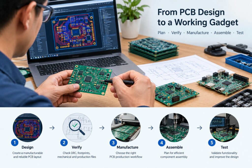
Creating a printed circuit board is a part of making gadgets. Finishing the PCB layout is the start. For the board to work well it has to go through steps. These include checking the design, getting ready, for manufacturing the board, putting parts on it and testing it.
Even a tiny mistake in any of these steps can cause problems. It might cost money, slow down development or make you redesign the board times. That’s why engineers and hardware developers should think about the production process when they design a printed circuit board. They should not just focus on the schematic and layout.
This article talks about the steps that turn a printed circuit board design from an idea into a working electronic product.
Start with a Manufacturing-Friendly PCB Design
A PCB must be designed with both performance and manufacturability in mind. The design choices, like trace width, copper spacing via size, hole size and component placement all influence how easy the board is to make and put together.
Before you route the PCB it is helpful to set design rules that match the expected electrical needs and how the board will be made. Small traces, tight clearances and complicated via structures might be needed for advanced projects but they should not be used without good reason. A design that leaves manufacturing margin is usually easier to produce every time.
Component placement matters well. Arrange the parts on the PCB to keep paths short spread power evenly manage heat and make assembly easy. Keep analog circuits away from noisy digital or high‑current zones when you can.
Engineers should think about how the finished PCB will be tested. Giving access to signals and power lines via test points can make debugging far easier, in the prototype phase.
A well‑planned layout cuts down on problems that must be fixed after the PCB is already made.
Verify the Design Before Creating Production Files
Before sending a PCB for production the complete design must go through a review.
The Design Rule Check is a starting point. It can find problems like clearances, unconnected nets overlapping objects and other layout violations.. A successful DRC does not mean the design is ready for manufacturing.
Important component footprints should also be checked against manufacturer datasheets. Pad dimensions, pin numbering, polarity, package orientation and thermal pad requirements need attention. An incorrect footprint can make a designed circuit hard or impossible to assemble.
Mechanical features should be checked too. The board outline, mounting holes, connectors, cutouts and enclosure clearances should all match the intended application.
Once the layout has been checked the manufacturing files should be. Looked at separately. Gerber files, drill data, board outlines and other production details should correctly show the PCB revision.
Using a Gerber viewer is a final step because it lets engineers look at the actual files that will be used during fabrication. This can show missing layers, wrong drill information or strange graphical parts that might not be clear, in the PCB design software.
Choosing the Right PCB Production Workflow
Choosing a PCB manufacturing service is not about the price. Engineers should look at what the factory can do, what board sizes and shapes it can make, what materials it offers, what assembly choices it gives, how it checks quality and how much help it gives with design.
The way you make boards should fit the stage of the project. In prototyping the aim is to test the circuit and spot design mistakes. In this phase a few boards are usually enough.
When the design is ready the focus shifts to making sure each board is the same, finding suppliers for components, speeding up assembly and ensuring long‑term reliability.
Today online manufacturing sites make this easier because engineers can upload files, pick board settings and move from prototype to production in a smooth flow.
Companies like JLCPCB are part of this growing network helping developers turn checked PCB designs into boards, for testing and more development.
No matter which manufacturer you choose, engineers must always read the design needs and production rules before sending the set of files.
Consider PCB Assembly During the Design Stage
PCB fabrication and component assembly are closely connected. Even if a board is fabricated perfectly it can still cause trouble during component assembly if the placement of components and the footprints were not planned correctly. I have seen boards fail because of this.
Surface-mount components need the pad shape and enough space for soldering. Fine-pitch devices, BGAs, QFNs and other small packages may need design care. I have noticed that designers sometimes overlook this.
Component orientation also affects how well assembly works. When it is practical placing components in the same orientation makes manual inspection and automated assembly easier. I have seen this improve inspection and reduce mistakes.
The Bill of Materials must match the PCB revision. Manufacturer part numbers, component values, package types and approved alternatives should be checked closely. Even a small component substitution can cause problems if the new part uses a footprint or has different electrical properties. I have seen substitutions cause big issues.
For automated assembly placement files must match the design. Component coordinates, rotation and which side of the board the part goes on should be verified before production. I have seen mistakes in placement files lead to delays.
Thinking about assembly needs early stops a situation where a made PCB cannot be assembled efficiently. I have learned that early planning saves time
Test the Prototype and Use the Results to Improve the Design
The first manufactured PCB is not the product; it is a step for engineering validation. We treat the PCB as a test board, not the finished item.
Start by testing the functions of the board. Verify that the power rails work, look for any circuits and confirm that the voltage levels are correct before installing or turning on any sensitive components. Then test each functional block separately.
For systems test the communication interfaces, clock signals, memory and peripheral connections. For circuits measure signal quality, noise levels, gain and frequency response.
Thermal behavior is also important in high‑current or power‑related designs. A board that works well for a period can still develop problems when components operate under continuous load.
Document the testing results. Use them to improve the next revision. Change component placement, routing, grounding, thermal management or mechanical features in the updated design.
This iterative process is a valuable part of hardware development. Each prototype provides information that moves the design closer, to an manufacturable final product.
Conclusion
Turning a PCB layout into a working gadget is no easy feat. You’ve got to pay attention at every step. The final design needs to work, be easy to make, simple to put together and pass all tests with flying colors.
Here’s the trick: think about how it will be made while you’re still designing it. Double-check all the details and the files you send to the factory. Plan how it will all come together.. Don’t forget, that first prototype is your best chance to learn. Get it right. You’ll save time and hassle later on.
The best dependable hardware isn’t just thrown together. It’s built through planning. From day one you’ve got to consider how it will be designed, made, assembled and tested. That’s the key to success.