Thinner and more fragile components have developed as a result of the increased demand for aesthetically thin electronics, which necessitates the use of dicing tape in their processing. Wafer component manufacturers are increasingly gravitating toward materials that offer high additive and impact strength, as well as curability that decreases when exposed to UV radiation. Companies in the global dicing tapes market are working on product innovation to incorporate films that are flexible and expandable, in order to meet these specific expectations of end consumers.
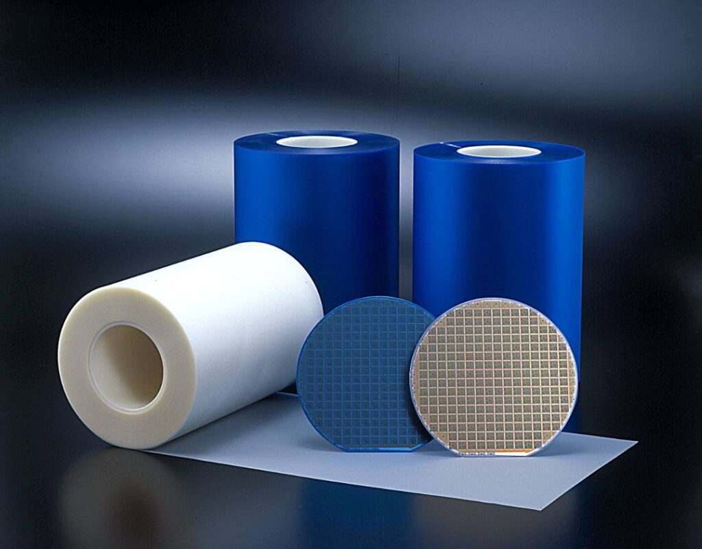
Dies and chips are separated from the semiconductor wafer during the wafer dicing process. Dicing tapes have a polyolefin, PVC, or polyethylene backing with an adhesive to keep the dies in place. There are two types of dicing tapes: UV film curable tapes and non-UV film or silicon free plastic films.
Extensive Use of Dicing Tapes in Multiple Applications to Spell Growth for the Market
Printed circuit boards (PCBs), integrated circuits (ICs), and other electronic components are in great demand. End consumers who employ high-performance small circuits in a variety of electronic devices are to blame for this. Dicing tape is used in the electronics industry to hold a piece of work together throughout the dicing process. Besides, the production of semiconductors and other electronic components are also expected to drive demand in the market. As a result, the demand for dicing tape is rising all around the world. Encapsulated package substrates, ceramics, silicon and GaAs semiconductors, glass, and crystals are just a few of the uses for this tape. To increase die quality, full-cut dicing of wafers requires dicing tape. Such extensive uses are anticipated to foster growth of the global dicing tapes market in the years to come.
Wafer thickness has been reduced as a result of technological breakthroughs and increased demand for attractively thin electrical goods. For the dicing procedure, wafer-processing businesses select materials with strong adhesive strength and UV curable tapes. Negative charges must be removed during back-grinding and dicing procedures for sensitive wafers. UV dicing tape and non-UV dicing tape are now used in PCBs (printed circuit boards), EMC package substrates, ICs, QFN (quad flat no-leads) & Si wafers, glass, ceramics, and lenses, amongst many other applications.
For Extensive Insights, Get PDF Brochure- https://www.transparencymarketresearch.com/sample/sample.php?flag=B&rep_id=46674