
How SEM And EDX Analysis Traces Manufacturing Defects That Standard Testing Misses

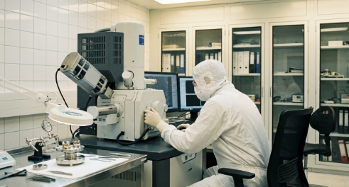
When a product defect cannot be explained by visual inspection or standard quality control methods, scanning electron microscopy with energy dispersive X-ray spectroscopy (SEM-EDX) provides the diagnostic resolution that closes the gap.
The technique images surfaces at magnifications exceeding 100,000x while simultaneously identifying the elemental composition of whatever appears under the beam, giving manufacturers both a picture and a chemical fingerprint of the failure.
What Does SEM-EDX Actually Do That A Regular Microscope Cannot?
SEM and EDX analysis answers two questions at once. The SEM component produces a high-resolution image of a material’s surface using a focused beam of electrons rather than visible light, reaching magnifications from 10x to over 100,000x with far greater depth of field than any optical microscope.
The EDX component identifies which chemical elements are present at the point of examination, producing an elemental spectrum that functions as a compositional fingerprint.
That combination is the point.
A standard optical microscope can show a quality engineer that a solder joint has cracked. SEM-EDX can show that the crack contains chloride residue from a contaminated flux, or that the solder alloy is tin-lead when the specification called for lead-free SAC305.
Optical microscopy sees shape. SEM-EDX sees shape and chemistry.
The distinction matters because most manufacturing defects that survive standard quality checks are compositional rather than visual. A coating looks intact but contains the wrong elements. A weld appears sound but has an oxide layer at the interface.
A foreign particle sits embedded in a product, and nobody can tell whether it came from the raw material, the machinery, or the packaging.
SEM-EDX answers those questions. Standard testing cannot.
Why Does This Matter For Manufacturers Right Now?
Product defects are becoming more expensive, not less.
Sedgwick’s 2026 State of the Nation US Product Safety and Recall Index recorded 3,295 recalls across five industries in 2025, with 858 million defective units removed from the market. That represented a 26 per cent increase in defective units compared to 2024.
US manufacturers paid $30.37 billion in product warranty claims in 2025, according to Warranty Week’s 23rd Annual Product Warranty Report. Rates ranged from 0.42 per cent of product sales for semiconductor companies to 3.5 per cent for some automotive manufacturers.
The pattern is consistent: defects that are caught late cost exponentially more to resolve. George Labovitz and Yu Sang Chang described this as the 1-10-100 principle in their 1992 book Making Quality Work.
A defect costs roughly $1 to prevent at the source, $10 to correct during production, and $100 to fix once it reaches a customer. The principle is an illustrative ratio, not an empirical constant, but the direction holds across every manufacturing sector.
SEM-EDX sits at the diagnostic stage. It does not prevent defects on its own. What it does is identify the exact cause of a failure with enough precision to direct corrective action at the right process, the right material, or the right supplier.
What Kinds Of Defects Does SEM-EDX Investigate?
Three categories account for most SEM-EDX casework in commercial laboratories.
Contamination and foreign particles. A metal fragment appears in a food product. Is it stainless steel from processing equipment or carbon steel from a structural component?
SEM-EDX determines the elemental composition (chromium and nickel ratios for stainless steel grades, for instance) and narrows the source from “somewhere in the factory” to a specific material type. SGS Institut Fresenius has documented SEM-EDX as a standard method for identifying inorganic particle contamination in food and pharmaceutical products.
Coating and plating failures. A coated automotive component blisters after six months in the field.
Cross-sectioning the part and examining it under SEM-EDX reveals the layer structure: coating thickness, interface adhesion, contamination between layers, and whether the coating composition matches the specification.
A zinc-nickel plating that was supposed to contain 12 to 15 per cent nickel but shows only 6 per cent has a bath chemistry problem. SEM-EDX confirms this in a single analysis session.
Material substitution and counterfeit components. A bond wire in a semiconductor package is specified as gold but EDX analysis reveals it is copper with a thin gold flash.
Mouser Electronics has cited SEM-EDX as a key technique in counterfeit electronic component detection programmes, particularly for identifying die material substitutions and incorrect alloy compositions that visual inspection cannot detect.
Each of these scenarios shares a common structure: something went wrong, the cause was not visible, and the answer required knowing what elements were present at the failure site.
How Does SEM-EDX Compare To Other Analytical Techniques?
SEM-EDX is one of several analytical tools available for failure investigation. Choosing the right one depends on the question being asked.
How SEM-EDX, optical microscopy, and XRF compare for defect investigation
| Attribute | Optical microscopy | SEM-EDX | XRF (X-ray fluorescence) |
| Magnification range | Up to approximately 1,000x | 10x to over 100,000x | Not an imaging technique |
| Elemental identification | No | Yes (point analysis, line scans, elemental maps) | Yes (bulk composition) |
| Spatial resolution | Limited by wavelength of light | Down to sub-micrometre | Typically 1 to 10 mm spot size |
| Sample preparation | Minimal | Conductive coating may be required; cross-sectioning for layer analysis | Minimal |
| Best suited for | Surface defects visible at low magnification | Identifying unknown particles, layer composition, interface contamination | Rapid screening of bulk material composition (RoHS, alloy verification) |
| Typical turnaround | Immediate (in-house) | 1 to 5 working days (commercial laboratory) | Immediate to same-day (handheld or benchtop) |
The table clarifies when each technique earns its place: optical microscopy for visible surface defects, XRF for rapid bulk screening, and SEM-EDX for cases where the defect is microscopic, compositional, or both.
ASTM International publishes standard practices for SEM-EDX analysis (ASTM E1508 for quantitative analysis by EDS), providing the methodological framework that accredited laboratories follow for reproducible results.
Where Can Manufacturers Access SEM-EDX Analysis?
SEM-EDX equipment is expensive. A new scanning electron microscope from manufacturers such as JEOL, Carl Zeiss, or Thermo Fisher Scientific costs between $200,000 and $2 million depending on configuration. Most SME manufacturers do not operate their own instrument.
Three access models exist.
Multinational testing groups including SGS, Intertek, and Bureau Veritas operate SEM-EDX capability across global laboratory networks. These providers offer broad accreditation coverage and established reporting formats, with turnaround times typically ranging from three to ten working days depending on workload and sample complexity.
University research laboratories at institutions such as Universiti Sains Malaysia (USM) and Universiti Kebangsaan Malaysia (UKM) operate SEM and FESEM instruments for academic and collaborative research.
Access for commercial manufacturers typically requires a research collaboration agreement, and turnaround times reflect academic scheduling rather than commercial urgency.
Independent commercial laboratories offer a middle path. Biochem Laboratories, an ISO/IEC 17025 accredited analytical laboratory headquartered in Penang since 1977, provides SEM-EDX and FESEM analysis for manufacturers requiring failure investigation and materials characterisation.
For manufacturers in Malaysia’s northern E&E corridor, a Penang-based laboratory eliminates the transit delays involved in sending samples to Singapore or Kuala Lumpur for analysis.
The choice between providers depends on the manufacturer’s specific need. A multinational exporter requiring globally recognised test reports may prefer SGS or Intertek.
A local manufacturer needing rapid turnaround on a contamination investigation may find an independent laboratory such as Biochem Laboratories (biochem.com.my) more responsive.
What Should A Manufacturer Do Before Sending Samples For SEM-EDX?
Sample preparation and context determine whether SEM-EDX analysis produces a useful answer or a technically correct but practically unhelpful report.
Three steps improve the outcome.
First, define the question before selecting the technique. “Analyse this sample” is not a question. “Determine whether the dark deposit on the connector surface is tin oxide, sulphide tarnish, or organic contamination” is a question. The more specific the brief, the more targeted the analysis.
Second, preserve the failure. Cleaning, handling, or modifying a defective sample before submission can destroy the evidence that SEM-EDX would otherwise detect. A contamination particle wiped from a surface is no longer available for analysis.
A corroded joint cleaned with solvent has lost its corrosion products. Submit samples in sealed containers with minimal handling.
Third, provide context. Tell the laboratory what the sample is, what it was supposed to be, what went wrong, and when the failure was first observed. A solder joint failure on a PCB that occurred after three months in a humid warehouse suggests a different investigation pathway than the same failure observed immediately after reflow.
Context guides the analyst to the right magnification, the right sample preparation, and the right comparison standards.
Experienced failure analysts consistently emphasise that the quality of the SEM-EDX result depends entirely on the quality of the question asked upfront; a vague submission produces a general elemental scan, while a specific question produces a diagnostic answer.
What Manufacturers Should Take From This
SEM-EDX does not replace standard quality control. It answers the questions that standard quality control cannot.
When a defect is visible, optical microscopy is sufficient. When a bulk composition needs rapid verification, XRF screening works. But when the question is “What is this particle made of?”, “Why did this coating fail?”, or “Is this component genuine?”, SEM and EDX analysis provides the answer in a format that directs corrective action at the source.
The technique has been available in commercial laboratories for decades. What has changed is the cost context. With product recalls reaching 3,295 events and 858 million defective units in 2025 alone, the cost of not identifying a defect’s root cause has never been higher.
A single SEM-EDX analysis session costs a fraction of a single warranty claim. For manufacturers dealing with unexplained failures, that arithmetic is worth considering.







Comment