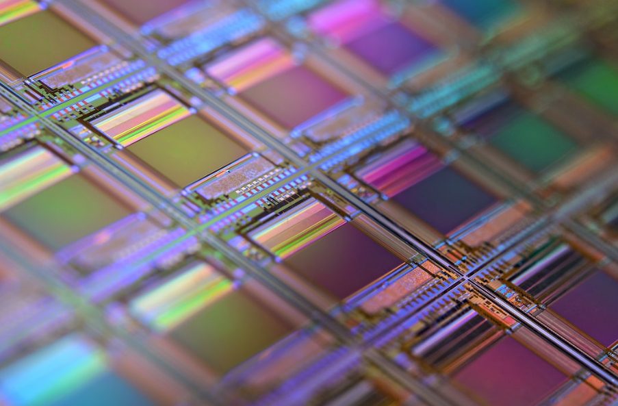
Patterned silicon wafers are essential in electronics manufacturing. They are thin slices of silicon with specific designs etched onto their surface. These designs guide the creation of circuits in devices like computers and phones.
Using patterned wafers improves efficiency and precision in production. Companies rely on them to maintain quality standards. Learning about these wafers helps engineers make better decisions.
If you want to understand how devices are built, explore patterned silicon wafers in more detail below.
The Manufacturing Process of Patterned Wafers
Patterned silicon wafers start as pure silicon crystals. These crystals are sliced into thin wafers. The wafers are cleaned to remove impurities.
Next, a pattern is applied using light or chemical processes. This pattern will define where circuits and components go.
Etching removes material from specific areas to create the design. Finally, wafers are coated to protect the patterns.
Each step requires precision to prevent errors. Understanding this process shows why quality control is critical.
Materials Used in Silicon Wafers
Silicon wafers are made from high-purity silicon. Other materials may be layered on the surface.
These layers can include metals or insulators. The combination allows circuits to function properly.
Choosing the right material ensures durability. Impurities can ruin the wafer’s effectiveness. Materials also affect the wafer’s electrical properties. Engineers must consider these factors during production. This careful selection leads to reliable devices.
Applications in Electronics
Patterned silicon wafers are used in computers, phones, and sensors. They guide the flow of electricity in circuits.
Microchips depend on these wafers for structure. Sensors in cars and machines use similar wafers.
Solar panels can also use patterned wafers for efficiency. They are part of many modern technologies. Devices would not work without these patterns.
Understanding their applications helps explain their importance. Engineers design patterns based on the intended use.
Quality Control Measures
Quality control ensures wafers meet strict standards. Wafers are inspected for defects after each step. Defective wafers can cause devices to fail.
Testing checks for electrical performance and surface accuracy. Precision tools measure thickness and patterns.
Companies follow strict guidelines to reduce errors. Cleanroom environments prevent contamination.
Maintaining high standards ensures reliable electronics. Regular monitoring is a key part of production.
Types of Patterns
Patterns vary based on device requirements. Some patterns are simple lines, others are complex grids.
Each pattern guides the placement of circuits. Designs affect how the final device will perform.
Engineers choose patterns to maximize efficiency. Some wafers are designed for high-speed circuits. Others are built for sensors or memory storage.
The pattern type influences the wafer’s cost. Choosing the right pattern is a critical step in manufacturing.
The Role of Etching
Etching shapes the wafer surface. Chemicals or light remove parts of the silicon. This creates grooves or raised areas.
Etching defines where electrical connections go. It must be precise to avoid errors.
Different etching methods are used for different patterns. The depth and width of etches matter.
Skilled technicians control the process carefully. Etching is essential to making functional wafers.
Lithography in Wafers
Lithography transfers patterns onto the wafer surface. It uses light or other methods to imprint designs.
The process is repeated for multiple layers. Alignment is critical to match patterns on different layers.
Small errors can cause circuit failures. Lithography allows high precision in production.
Engineers adjust exposure times and materials for accuracy. This step defines the final shape of the circuits. Lithography is a cornerstone of wafer manufacturing.
Cleaning and Preparation
Wafers must be cleaned at every stage. Dust or particles can ruin patterns. Cleaning involves chemicals and water in controlled environments.
Wafers are dried carefully to avoid damage. Preparation includes coating with protective layers.
Handling requires gloves and special tools. Proper cleaning increases yield and reduces defects.
Every wafer must meet strict cleanliness standards. This ensures consistent performance in devices.
Testing and Inspection
Testing checks the wafer’s electrical and structural properties. Tools measure conductivity, pattern accuracy, and surface defects.
Faulty wafers are removed before use. Inspection ensures the long-term reliability of devices.
Multiple tests may occur at different production stages. Advanced cameras and microscopes detect tiny flaws. Engineers use the data to improve production.
Regular testing prevents costly failures. Quality assurance depends on thorough inspection.
Handling and Storage
Wafers are fragile and need careful handling. Special carriers prevent damage during transport.
Storage requires controlled temperature and humidity. Mishandling can cause scratches or contamination.
Protective coatings reduce surface damage. Engineers follow strict procedures for movement. Proper storage maintains quality until use.
Handling protocols reduce waste. Safe practices ensure wafers are ready for production.
Innovations in Patterned Wafers
Patterned silicon wafers continue to improve. New techniques allow smaller and more precise designs.
Advanced materials enhance performance and durability. Innovations reduce production costs over time.
Research focuses on better patterns for faster devices. Engineers experiment with multi-layered wafers. Environmental impact is also a consideration.
Improvements expand applications in electronics. Staying updated is essential for manufacturers.
Integration in Electronics
Patterned silicon wafers are integrated into circuits and chips. They provide the foundation for electrical connections.
Devices cannot function without them. Engineers assemble wafers with other components.
The integration must align patterns accurately. Even a small misalignment can cause device failure. Some production lines focus on wafer integration efficiency.
Using patterned silicon wafers allows for consistent and reliable electronics. This process is key to modern technology.
Common Challenges with Patterned Wafers
Working with patterned wafers can be difficult. Wafers are thin and easy to break. Dust or small particles can ruin them quickly.
Patterns must line up perfectly each time. Etching mistakes are common if steps are rushed.
Some wafers crack during handling or transport. Cleaning too roughly can damage the surface.
Engineers need careful attention at all stages. Overcoming these challenges ensures wafers work correctly in devices.
Learn About Patterned Silicon Wafers
Patterned silicon wafers are a core part of electronics manufacturing. They guide the creation of circuits and components.
High-quality materials and precision processes are essential. Each step, from cleaning to integration, affects performance.
Innovations continue to make wafers smaller and more efficient. Proper handling and testing ensure reliability. Understanding patterned silicon wafers helps explain how modern devices work.
To read more, visit our blog page. We’ve got more topics!