A multilayer PCB is a printed circuit board that has multiple layers of conductive material. These layers are separated by insulating material. Multilayer PCBs are used in a variety of electronic devices, such as cell phones, laptops, and servers.
Benefits of multilayer PCBs
The main advantage of a multilayer PCB is that it can accommodate more circuitry than a single-layer PCB. Additionally, multilayer PCBs can be designed to have better electrical properties than single-layer PCBs. For example, multilayer PCBs can have better impedance control and better signal integrity click here for more.
Another advantage of multilayer PCBs is that they can be more compact than single-layer PCBs. This is because the multiple layers of conductive material can be stacked on top of each other. Additionally, multilayer PCBs can be designed with blind and buried vias, which are vias that do not go all the way through the board. This can further reduce the size of the PCB. Multilayer PCBs are more expensive than single-layer PCBs, but the extra cost is often worth it for the increased functionality and performance that they offer.
How to find a reputable multilayer PCBs supplier
When it comes to choosing a reputable multilayer PCBs supplier like https://uetpcb.com/, there are many factors that you need to take into account. In this blog post, we will share with you some tips on how to choose the right supplier for your needs.
The first thing that you need to do is to check the supplier’s credentials. Make sure that the supplier is registered with the Better Business Bureau or other similar organizations. You can also check online reviews to see what other customers have to say about the supplier.
The second thing that you need to do is to ask for quotes from different suppliers. This will help you compare the prices and services offered by different suppliers.
The third thing that you need to do is to ask the supplier for samples of their products. This will help you check the quality of their products.
The fourth thing that you need to do is to visit the supplier’s factory. This will help you see the manufacturing process and the working conditions of the employees.
The fifth thing that you need to do is to check the payment terms of the supplier. Make sure that the supplier offers flexible payment terms so that you can easily afford their products.
These are just some of the things that you need to take into account when choosing a reputable multilayer PCB supplier. By following these tips, you can be sure that you will find the right supplier for your needs.
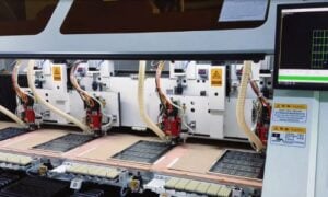
Multilayer PCB manufacturing process
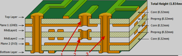
Multilayer printed circuit boards are made by bonding together multiple layers of conductive material. These layers are separated by an insulating material known as the core. The number of layers in a multilayer board can range from two to twelve, although most boards have four to six layers.
The conductive material used in multilayer PCBs is typically copper, although other metals such as aluminum can also be used. The copper is typically clad with a thin layer of solder resist, which helps to protect the copper from oxidation and corrosion.
The first step in the multilayer PCB manufacturing process is to create the individual layers that will make up the finished board. Each layer is created by bonding a sheet of copper to an insulating substrate. The substrate can be made from a variety of materials, but the most common are FR4 and polyimide.
Once all the layers have been created, they are then laminated together under heat and pressure. This process bonds the layers together and creates a strong bond between the conductive and insulating materials.
After the board has been laminated, it is then drilled so that holes can be created for the through-holes. The drilling process is followed by a plating process, in which a thin layer of metal is deposited on the walls of the through-holes. This metal helps to connect the different layers of the board.
Finally, the board is finished by applying a solder mask and silkscreen printing. The solder mask is a thin layer of polymer that helps to protect the exposed copper circuitry from damage. Silkscreen printing is used to add labels and other information to the board.