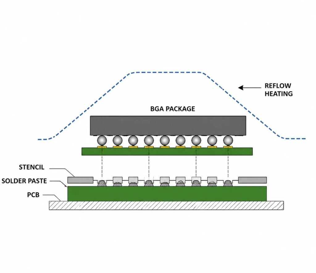
Shenzhen, China — Weller PCB is sharing engineering insights into the challenges of fine-pitch BGA PCB manufacturing, focusing on how advanced package requirements, PCB layout decisions, and assembly process control influence product reliability.
Fine-pitch BGA packages are widely used in processors, FPGAs, networking devices, embedded computing platforms, and other high-density electronic systems where more I/O connections are required within limited PCB space. As package pitches continue moving toward smaller dimensions, including 0.65 mm and 0.5 mm pitch designs, PCB manufacturers and engineering teams must carefully manage routing density, fabrication accuracy, and assembly consistency.
Weller PCB has published a technical resource covering Fine-Pitch BGA PCB Design, providing practical guidance on layout considerations, manufacturing requirements, and design decisions that affect BGA assembly reliability.
Addressing Fine-Pitch BGA Design Requirements
Unlike traditional component packages, fine-pitch BGA devices require precise coordination between PCB design and manufacturing processes.
- Key engineering considerations include:
- BGA pad geometry and solder mask definition
- Escape routing strategy beneath the package area
- Via structure selection and placement
- HDI stackup planning
- Signal and power distribution
- PCB fabrication tolerances
For higher-density BGA packages, conventional through-hole via structures may not provide enough routing space for all required connections. Engineers often evaluate HDI PCB structures and laser-drilled microvias to create additional routing channels while maintaining electrical performance and manufacturing reliability.
The transition from design concept to production requires close cooperation between PCB designers and manufacturers to ensure that routing strategies, layer structures, and fabrication capabilities are aligned.
Manufacturing Control Behind Reliable BGA Assembly
A successful fine-pitch BGA design depends not only on PCB layout but also on the consistency of fabrication and assembly processes.
- Manufacturing factors that influence BGA reliability include:
- Layer registration accuracy
- Copper distribution and plating control
- Surface finish selection
- Solder paste printing accuracy
- Reflow profile management
- Inspection capability
Because many BGA solder joints are hidden beneath the package, traditional visual inspection methods may not be sufficient. Advanced inspection methods such as X-ray inspection are commonly used to evaluate solder joint quality and identify potential assembly issues.
Through its fine-pitch assembly support, Weller Technology Co. Ltd. works with customers on PCB assembly requirements, manufacturing coordination, engineering communication, and production preparation for complex electronic applications.
Improving Design-to-Production Collaboration
Many challenges in advanced PCB manufacturing can be reduced when engineering teams and manufacturing partners communicate early in the development process.
Important discussions before production may include:
- Component package requirements
- BGA escape routing limitations
- PCB stackup configuration
- Assembly process capability
- Prototype validation requirements
“A fine-pitch BGA design is not only a layout challenge; it is a manufacturing collaboration challenge,” said Kevin Duan of Weller Technology Co. Ltd. “When design requirements and production capabilities are evaluated together, engineers can achieve better manufacturability and more predictable results.”
Weller PCB continues to support OEMs, hardware developers, and engineering teams working on high-density electronic products that require reliable PCB manufacturing and assembly performance.
About Weller Technology Co. Ltd.
Weller Technology Co. Ltd. is an engineering-focused PCB manufacturing and electronic manufacturing solutions provider based in Shenzhen, China.
The company works with OEMs, hardware developers, and engineering teams requiring PCB fabrication support, PCB assembly capability, manufacturing coordination, and technical collaboration throughout the product development process.
Weller PCB supports customers with PCB manufacturing, assembly services, engineering review, and production coordination, helping transform complex electronic designs into reliable and manufacturable products.
By combining manufacturing experience with engineering communication, Weller Technology Co. Ltd. focuses on improving manufacturability, quality consistency, and production reliability for demanding electronic applications.
Media Contact
Kevin Duan
Weller Technology Co. Ltd.
Email: [email protected]
Address:
4/F, Bldg.3, Huafeng Longgang Overseas Returnees Ind. Park,
Baolong 1st Rd, Nanyue Community, Baolong Street,
Longgang District, Shenzhen, Guangdong, China
Postal Code: 518116
LinkedIn: Weller PCB
https://www.linkedin.com/company/wellerpcbs/