Consistent turns of events and execution of new advances, for example, natural substrate-interposer innovation and silicon-through interconnection innovation in the semiconductor assembly and testing services market are setting out huge income open doors for players in the semiconductor assembly and testing services market. Execution of semiconductor assembly and testing services in the purchaser gadgets area assists makers with creating semiconductors, memory chips, and wafers utilized in shopper electronic items and remote/portable handsets in a more effective way.
The worth of the worldwide semiconductor assembly and testing services market is expected to observe a CAGR of 5.8% during the gauge time of 2019-2029.
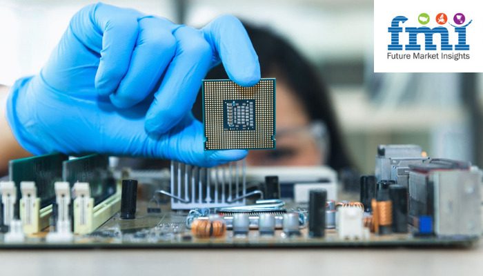
Key Takeaways of Semiconductor Assembly and Testing Services Market Study
- Among the application section, buyer hardware fragment is relied upon to observe high development rate, inferable from rising interest for sound/video gear, cameras, number crunchers, and shrewd homes (home wellbeing gear and adornments)
- Asia Pacific Excluding Japan is relied upon to set out worthwhile development open doors for players in the semiconductor assembly and testing services market, owing to fast development of bundling of semiconductors, and expanding uses of semiconductor assembly techniques around here
- Expanding interest for associated gadgets overall including cell phones and tablets having availability and interactive media abilities moves interest for higher bundling innovations and sets out development for specialist organization.
More appeal for versatile and associated gadgets like tablets and cell phones, has supported the interest for higher bundling advancements. Additionally, rising interest for advanced video content drives development of superior execution and portable buyer hardware items, for example, Wi-Fi chipsets and other semiconductor chips. For example, STATS chipPAC (JCET) creates extended Wafer Level Chip Scale Package (eWLCSP), which offers further developed testing and a minimal expense fan-in wafer level bundle for space-controlled cell phones.
ODMs and OEMS to Prioritize ‘Fab-light’ Strategy
As semiconductor process innovation moves to bigger wafers and more modest component sizes, cost of building cutting edge wafer manufacture plants has risen essentially, arriving at a few billion dollars. High speculation costs for cutting edge silicon innovation and hardware are impacting different semiconductor organizations to take on or keep a ‘fabless’ or ‘fab-light’ technique. The expanding interest for semiconductors are required for cloud reconciliation and availability with including sensors, processing, intuitiveness and specialized gadgets.
Insights on Semiconductor Assembly and Testing Services Market
FMI’s report on the semiconductor assembly and testing services market is divided into three significant areas like services (assembly and bundling services (copper wire and gold wire holding, flip chip, wafer level bundling, TSV, others), and testing services), applications (interchanges, registering and organizing, customer hardware, modern and auto gadgets, and locale to assist perusers with understanding and worthwhile assess potential.
Get a Sample Copy of the Report