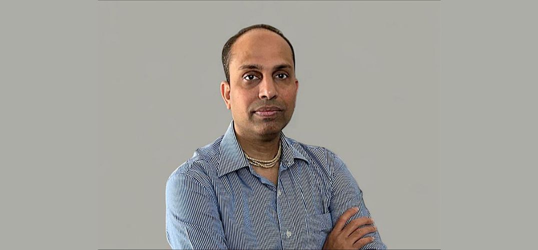
In semiconductor design, even the tiniest error can lead to a chip that doesn’t work. This can cost companies millions of dollars and waste significant time. For this reason, the verification process is essential—few are as skilled at this task as Prashanth Paladugu.
Paladugu has worked on VLSI (Very Large Scale Integration) for over 15 years. As a testbench architect at one of the major semiconductor manufacturers, he is changing how semiconductor verification is done. He employs the latest tools and techniques and dedicates himself to being as accurate as possible.
Paladugu’s primary tool is the Universal Verification Methodology (UVM), a widely applicable set of standards that allows him to test designs thoroughly in an open-ended manner. Every detail is checked to ensure there are no bugs or errors. To Paladugu, verification is not just a job; it’s a responsibility to society.
The stakes are high. According to Deloitte, the global semiconductor market is expected to reach $588 billion in 2024, growing from $520 billion in 2023. With such a high demand for reliable semiconductor devices, Paladugu’s skills are more valuable than ever.
Taming Complexity
As the semiconductor field continues to cram more transistors onto ever-smaller chips, the devices’ complexity has skyrocketed. Traditional manual verification methods have struggled to keep pace with this exponential growth. Fortunately, Paladugu’s mastery of advanced verification techniques allows him to handle even the most complicated designs.
His hands-on experience covers an array of IPs, from the esoteric (WIFI-PHY, PCIE, PCS, MIPI) to the familiar (USB, AXI, AHB, APB, UART, I2C, JTAG). This broad expertise allows him to create comprehensive test plans for the current VIPs, covering all possible scenarios and ensuring the complex system-on-chip (SoC) designs are thoroughly validated.
“Though I’ve solely been working as a consultant for several years now, I’ve encountered many other positions that demanded various technical skills. Implementing functional coverage, Python scripting, cross-verification across designs—it’s a big industry,” Paladugu states.
Methodical Verification Approach
Paladugu’s approach to verification is both systematic and meticulous. His implementation of functional coverage stands at the core of his methodology, enabling him to identify valid gaps in the testbench that require additional constraint random directed tests. This strategic approach ensures comprehensive verification rather than merely running predetermined test cases.
“The functional coverage that I do ensures that if there are any valid holes in the test bench that would help me to write more constraint random directed tests,” Paladugu explains. “While the regression gives the overall code coverage and functional coverage.“
His verification standards are exceptionally rigorous. Paladugu aims for code coverage without exclusions to reach at least 99% and often achieves 100%—a testament that the entire specification of the verification IP is thoroughly covered. This level of thoroughness provides confidence that designs are ready for tapeout, the final step before implementation of the physical design.
Perhaps most critically, his expertise with constraint random stimulus using UVM verification methodology helps detect bugs that might otherwise slip through conventional testing methods. “The most critical of all of them is through constraint random stimulus using UVM verification methodology, which helps me detect critical bugs that if ignored, can cost in millions of dollars,” Paladugu notes.
Fostering Collaboration
In a field where communication can be difficult, Paladugu champions collaboration. He is known to have worked alongside other teams on the integration of IP (Intellectual Property) at the major semiconductor manufacturer. He holds a reputation for being a mentor with a remarkable ability to unite people.
He maintains good relationships with colleagues across different teams, breaking down barriers and enabling cross-functional collaboration, essential for driving efficiency in semiconductor manufacturing.
Paladugu also strongly supports new methodologies like the Portable Stimulus Standard (PSS), which aims to make verification more standardized, reusable, and automated.
Setting New Standards
As the semiconductor sector hurtles towards a projected $1 trillion market size by 2030, according to McKinsey analysis, pioneers like Prashanth Paladugu are becoming ever more critical. His focus on accuracy and thoroughness sets a new standard for the industry, helping keep pace with the rising demand for more silicone chips.
What sets Paladugu apart is not just his technical expertise but also the comprehensive scope of his responsibilities. He single-handedly manages the entire verification workflow that would typically require a team of five to six specialists.
His responsibilities encompass verification plan development, building complete reusable advanced testbench architecture, building verification environments from scratch, developing Bus Functional Models (BFMs), developing end to end complex test scenarios, conducting thorough coverage analysis, and ultimately signing off on verification—all critical steps that ensure semiconductor designs function flawlessly.
“I do the entire test bench architecture, building from scratch. I develop the Bus Functional Model (BFM) and do the complete coverage analysis and am also responsible for the verification signoff,” Paladugu shares. “All this by one person requires a deep understanding of the methodology, experience, and core skills–something not always possible.“
His work contributions to the broader semiconductor community ensure that the devices that power an increasingly connected world are reliable and up to the task.


