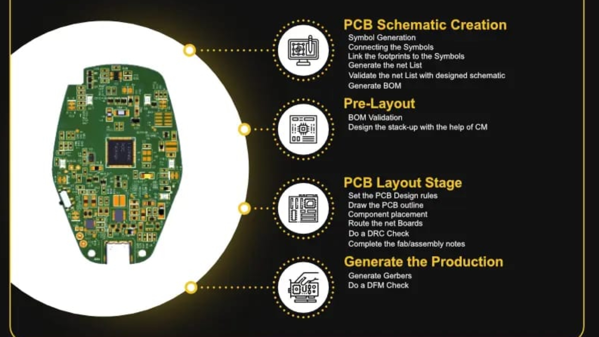
The electronic devices are established based on PCB Design Services. These services bring ideas into working circuit boards. Special software is used with design layouts by engineers. They insert parts and connect them with copper traces. The PCB design between concept and real-life product.
The circuit board that allows your smartphone to work was a perfect design by somebody. The next time you make a call, reflect on this !! Behind each electronic wonder, there is a masterful piece of PCB design work. Smart companies invest in professional PCB services early. Such investment is reimbursed in the form of superior products and satisfied customers. The PCB design services are what can make your most ambitious technical fantasy come true.
Design services for PCB assist in transforming an idea into a real product. They are the people who apply electronic notions to the real world. These services are the medium between creativity and invention.
What are PCB Design Services?
Take your most loved gadget and think of it as a carcass PCB. It also ensures that there is a flow of electricity in the right direction. Then, engineers work this idea into a functioning circuit board. The craft is time-consuming and requires. The outcome is a board that brings your machine into perfect operation. The PCB planning is conducted by the special software utilized by the PCB designers. It also aids them in connecting all of these with thin copper wires called traces. This illustrates how all the parts are electrically connected. Next will be the layout design. Last is the testing and verification.
Why PCB Design Matters
Many issues are averted with good PCB design. Mal-design may lead to devices breaking down. It can even render them unsafe as well. Pro designers are familiar with how to design to avoid such problems. PCB design affects device performance. A well-designed board makes devices run faster. It also makes them use less power. Size matters in electronics today. Everyone wants smaller devices. Good PCB design makes this possible. Price is never a small matter. It also minimizes the faulty products. This is cost cost-saving to both firms and clients.
Custom pcbs Solutions
Each electronic machine requires special demands. Standard products rarely work. Here custom PCB design stands forth. Custom design begins with knowledge. What should the device that must do? What is the biggest size that it can be? What amount of power does it have to use? The first questions to be asked by the designers are listed below.
Selecting materials is a major concern. Various applications require various materials. Biocompatible materials are required in medical devices. The electronics in cars require heat-resistant materials. Designers are familiar with what materials are most effective. The functioning of parts properly arranged is more efficient. They are also less heat-generating.
Types of Custom Designs
The most simple are single-layer boards. One side only of then have any components. Such boards are suitable for simple applications. They are also the least costly to produce. More complicated are multilayer boards. They possess circuits in layers. This enables connections to be established in a small area. All modern devices are run on multi-layer boards. Flexible PCB is easy to bend and twist. They are good at wearable watches. They also appear in crammed spaces better. There are inflexible component places. This provides more choices to a designer.
PCB Prototyping Service
Prototyping is the production of real pieces of paper. It is where the notions become actual. Enter prototypes to work and test designs before going into mass production. Prototypes have a fast turnaround. Designers will demand quick feedback on their ideas. Small quantities are perfect for testing. Multiple iterations are normal. The prototype rarely works perfectly. Each iteration improves the design. Most products go through 3 to 5 prototype cycles.
Benefits of Prototyping
Risk reduction is the biggest benefit. Prototypes reveal problems early. Fixing problems in prototypes costs much less than fixing them in production. Performance validation ensures designs meet requirements. Real testing beats computer simulation every time. Mechanical fit can be tested with prototypes. Components might not fit as expected. Prototypes reveal these issues before expensive tooling is made. Team feedback improves designs. When people can hold and test a prototype, they provide better input. This leads to better final products.
Manufacturing Considerations
Manufacturing should be considered at the design stage of the PCB. Good-looking designs on paper may be difficult to construct. Designs that are friendly in manufacturing are cheaper and effective. Component availability affects design choices. Designers choose widely available components when possible.
Assembly methods influence design rules. Some components need special handling. Others require specific temperatures. Good designers know these requirements. Testing access is important. Finished boards need testing before shipment.
Quality and Standards
PCB design follows strict industry standards. These standards ensure compatibility and safety. They also help manufacturers worldwide work together. IPC standards govern most PCB design rules. These standards cover everything from trace width to hole sizes. Compliance with norms will provide a guarantee of the quality of production
Quality planning takes place through good design. Boards with fewer defects are well designed. They can also test more readily. Quality in the design saves money down the road. Certification might even have to be done on certain products. The medical equipment, car electronics, and aerospace have unique demands.
The Future of PCB Design
With the advancing technology, it is fast and increasing. New trends have to be taken into account in CB design services. Designers are beginning to be aided by artificial intelligence and machine learning. Miniaturization is ever driving towards frontiers. Each year, components are becoming tinier. CB design will have to accommodate small components and interconnections. Environmentalism informs analyses of design decisions. Soldering without lead is now the norm. Recycling is catching up, and using more recyclable materials is on the rise.
Green design practices are growing.
5G and IoT devices create new challenges. These applications need special antenna designs. They also need ultra-low power consumption. PCB designers are learning these new skills.
Conclusion:
PCB designs services create the invisible foundation of our connected world. All our smart devices, all the computers, and any electronic gadget would be useless without properly developed circuit boards. These services are used to bring innovative ideas into the type of technology that forms the people of each day.
The next time you turn on your smartphone or your laptop, bear in mind the brilliant designers, who made it happen. They have solved so many technical puzzles to develop the miniature circuit board within. Their competence will guarantee you the reliability of the day-to-day working of your device.
The PCB design services will keep modifying and innovating ever-advancing technology. They will continue to stretch the potential of electronic technology. It is with the system boards they are designing now that the future of technology hangs.