All the electronic and electrical manufacturers are trying to provide high-quality products with the best performance to the market. So, this achievement needs to meet all design standards and rules related to electronic systems. Electronic devices must have the required standards and certificates to access the markets.
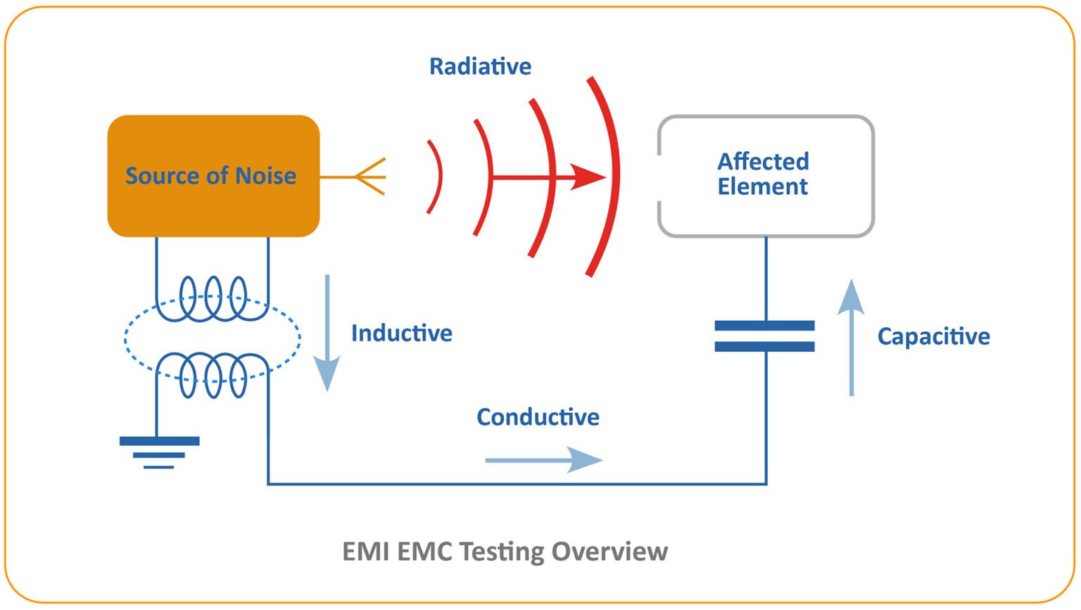
One of the crucial subjects that would be considered in electronic systems design is EMI/EMC testing and standards. The concept of Electromagnetic Interference EMI refers to the noise signals of an electronic circuit that interfere with nearby devices and cause disturbances in the device’s operation.
Electromagnetic Compatibility EMC is the electronic circuit’s capability to operate correctly and efficiently under interference noise signals.
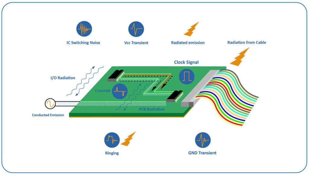
EMI resources
If we return to the physics lesson and remember Faraday’s law, according to this rule, any wire and electronic component that carry electrical current produces an electromagnetic field around itself. The extensive electromagnetic energy causes harmful effects on the operation of nearby devices. The measure of the Electromagnetic field is related to the rate of changes in the coil area and the current. So, EM emission increases with the rise of each of these factors, loop/coil area, or the rate of current changes.
Impedance mismatching in the circuits is the most effective element in EMI problems. Mismatched impedance from a source to a destination increases reflections. Hence, radiative emission increases.
Also, High-frequency traces and Poor capacitance decoupling produce unintentional current and EM emissions.
Switching circuits such as the clock signal and the high-rate transmission signal provide EMI problems.
PCB design for EMC compliant
A proper EMC-compliant board should have three characteristics: it doesn’t interfere with other
boards, has immunity against the emission of other systems, and even doesn’t interfere with its operation.
To meet the above specifications and the best PCB design to reduce EMI, knowing the sources of EMI helps to choose the minimization EMI methods for specific sources.
We can define the sources of EMI in three Parts: electronic Components, PCB Layout, and External EMI Sources. And each of them uses specific methods for EMI reduction.
Guideline for component EMI:
Electronic components that have high power consumption, such as transmitters, antennas, and switching components, generate EM emissions.
Some precautions to limit EMI associated with electronic components:
- Select the low-power consumption components
- Use of SMD (surface mount devices) instead of through-hole devices. SMD obtains lower resistance and inductance, limits the effect of RF energy, and is suitable for high-frequency applications.
- Grouped and isolated the same processing signal component from the different types of components, for example, digital components located nearby together and isolated from analog components.
- Isolate electronic components or sub-circuits with a Faraday cage. Faraday cage is an enclosure that protects sensitive electronic components from EMI and adds the ground to the PCB. Also, prevent radiation emission into the environment around the board.
Guideline for PCB layout EMI:
Observing some notes on the design Traces, Ground Plane, PCB layers arrangement, Shielding, grouped sensitive components, Decoupling capacitor, and Controlled impedance can reduce the EMI problems in printed circuit boards.
Traces
Traces are conductive paths on the surface of the PCB to flow electricity current and transfer signals between the electronic components. Traces should be made of material with high electrical conductivity and stability. Copper is the most common metal used for trace material. Sometimes use aluminum and even gold in making traces.
Traces have the ability to function as a radiating antenna and cause radiated or conducted emissions in circuit boards.
Tops tricks for design trace layout
- Trace separation or clearance: All signal traces, including high-speed, low-speed, analog, and digital signals (high-speed traces: clocks, video, audio, reset, etc.), must be separated from each other. Also, trace spacing and clearance distance should be based on IPC standards. Generally, spaces between the traces should be the third time (3W) of the trace width.
- Uses of differential signal pairs: Differential signaling is a technique for transmitting an electrical signal by employing two complementary voltage signals with an opposite polarity that send in a pair of conductors. Every differential signal needs to have two traces lined up side-by-side.
The advantage of using differential signal pairs is to reduce electromagnetic interference from other noisy traces. Because of negative and positive polarity signals with the same voltage, the EMI reduces both noise emission and noise acceptance.
Differential signals can operate at lower voltages than single-ended signals, so we benefit from low power consumption and result in reduced EMI.
- Angles: Sharp angles in traces result in an increase in capacitance and result in a change in characteristic impedance value and growth in reflection. Try to use 45° turns instead of 90° bends.
- Vias: Vias are used in multi-layer PCBs for signal routing purposes. Try to use vias wisely. Because vias have their capacitance and inductance effect on the PCB. And professional Designers should be aware that the capacitance and inductance in the vias provide an impedance mismatch between via and trace, which creates reflections.
Where to force the use of vias, such as in differential pairs, should be located at ground vias and signal vias near each other. In this state, the characteristic impedance value will be controlled, and then it eliminates reflections.
- Clock circuits:
Clock signals as high-speed signals naturally propagate EM emissions, and guard and shield traces for clock lines and circuits help their immunity from receiving and sending EM emissions. Shielding and guarding traces cues to reduce inductive and capacitive coupling that limited the scattering noise along the power path.
Ground plane
The Ground Plane on PCB is a large copper-filled area that is connected to the circuit Ground. Sometimes a small part of the board is in a one-layer or two-layer PCB, and or allocates one entire board layer to itself in multi-layer boards.
One of the most important ground plane tasks, in addition to voltage and signal return, is to reduce noise and EM interference. A Ground with low inductance is the advantage of a good Ground Plane design for low EM emission. Ground Planes with a large conducting area have lower impedance against digital circuit switching and help to reduce noise pulses.
- Minimizing signal return paths: The signals’ return path through the ground makes a loop that produces impedance, and this longer loop provides higher impedance due to failure in EMC performance. So, try to optimize the signal return path.
- Connect to ground the copper-filled areas: To prevent copper-filled areas from acting like antennas and causing EM problems should be connected to the ground. The copper-filled area is used for thermal conductivity.
PCB layers arrangement or stacks up
Layer arrangement in multilayer PCB impacts EMC performances. For best EMC performance, it’s recommended to have a structure and proper sort of signal layer, power layer, and ground layer.
In PCB stack-up, avoid locating conducting layers next to each other and divide them by a ground plane.
Decoupling and bypass capacitors
High-speed circuits use the decoupling capacitance technique to reduce EMI in power rails. Switching high-frequency current in ICs with high-speed application generates radiated emissions and thus EMI. Therefore, use a bypass capacitor and connect it to the ground planes.
Impedance matching and minimized high-frequency ringing
Ringing is an unwanted oscillation that is not on the design map and occurs due to parasitic capacitances and inductances generated by an electrical signal in the circuit. In high-frequency circuits, mismatching impedance between the source and destination makes high-frequency ringing and signal reflection. Increased RF energy from reflection and ringing produces radiated or conducted emissions in the circuits, resulting in an EMI problem. The easiest way to obtain impedance matching is by using RF termination techniques.
Shielding
Shielding can help to protect the board from external EMI. A shield is an enclosure made of conductive or magnetic materials. It is utilized to cover the entire board or a part of it and connected to the ground. Shielding by arresting and reflecting a part of antenna radiation effectively helps to decrease the antenna’s loop size.
Cable shielding
A shielded cable or screened cable acts as a Faraday Cage. And it prevents interference from external noise onto the cable signal and also the signal noise radiating out to other components and provides a good EMC performance.
Different types of signals like digital, analog, and high-frequency signals generate EMI issues because of their parasitic capacitance and inductance elements. The best way to limit EMI for these signals is to use a shielded cable and ground the shield at both the front and back cables so that these signals can limit the EMI.
Conclusion
For best EMI/EMC performance, you should consider many accurate notes and applicable rules in PCB design. It is clear that it couldn’t eliminate the EMI, but it can be minimized by appropriating the EMI design rules.
Finally, an electronic device, after all the PCB design process and test engineering for promotion to any geographical market required to pass EMI standards and certifications related to that country. For the USA, the approval certification for RF emissions is FCC compliance. The authorization standards and rules for RF devices are prepared in part 47CFR part 2.
Author: Sherry Mosleh IoT Development Engineer at Arshon Technology Inc.