Introduction to PCBA (Printed Circuit Board Assembly)
Welcome to the fascinating world of the PCBA (Printed Circuit Board Assembly) manufacturing process! Have you ever wondered how those intricate circuit boards inside your electronic devices come to life? Join us on a journey behind the scenes as we unravel the magic of turning raw materials into functional PCBAs. From design to testing, packaging, and shipping – let’s dive deep into the meticulous process that brings technology to your fingertips.
The Manufacturing Process: Pre-Production
In the pre-production phase of PCBA manufacturing, several crucial steps take place to ensure a smooth assembly process. First and foremost, designing the PCB layout is essential for determining component placement and connectivity. Engineers meticulously plan the circuit design using specialized software to optimize functionality.
Once the PCB layout is finalized, procuring components comes into play. This involves sourcing all necessary electronic parts from trusted suppliers to guarantee quality and compatibility with the board. Attention to detail during this stage is paramount to avoid any delays or issues down the line.
After the components are secured, the solder paste application takes center stage. The precise deposition of solder paste onto designated pads prepares the board for component attachment during later stages of production. This meticulous process sets the foundation for successful PCBA assembly.
A. Designing the PCB layout
Designing the PCB layout is a crucial first step in the PCBA manufacturing process. It involves strategically placing components on the board to ensure optimal functionality and efficiency. Engineers use specialized software to create a digital blueprint of the circuit, considering factors like signal integrity and thermal management.
The layout must be carefully planned to minimize signal interference and ensure proper electrical connections. Components are positioned based on their functions, sizes, and heat dissipation requirements. The designer must also consider factors like trace length, component orientation, and potential EMI issues.
Once the initial design is complete, it undergoes rigorous testing and verification processes to identify any potential issues before moving to production. Design revisions may be necessary to optimize performance or address any unforeseen challenges that arise during testing.
Designing the PCB layout requires a combination of technical expertise, creativity, and attention to detail to create a reliable and efficient circuit board for PCBA manufacturing.
B. Procuring components
When it comes to PCBA manufacturing, procuring components is a crucial step in the process. This involves sourcing all the necessary parts and materials required for assembling the printed circuit board.
To ensure smooth production, manufacturers need to establish strong relationships with reliable suppliers who can deliver high-quality components on time. This includes electronic components such as resistors, capacitors, and integrated circuits.
Procuring components also involves thorough quality checks to guarantee that each part meets the specified requirements and standards. Any substandard or counterfeit parts can jeopardize the performance and reliability of the final product.
Efficient inventory management plays a key role in ensuring that all components are readily available when needed during the assembly process. Manufacturers must carefully plan their component procurement strategies to avoid delays or shortages that could impact production timelines.
Meticulous attention to detail and effective communication with suppliers are essential for successful component procurement in PCBA manufacturing.
C. Solder paste application
Once the components are procured, the next step in the PCBA manufacturing process is solder paste application. This crucial step involves applying a thin layer of solder paste onto the PCB using a stencil. The stencil ensures precise placement of the solder paste on specific areas where components will be attached.
Solder paste is a mixture of tiny balls of metal alloy and flux. The flux helps to clean and prepare the surfaces for soldering while holding the metal particles in place until they are heated during reflow. The amount and placement of solder paste must be accurate to ensure proper connections between components.
After applying the solder paste, automated equipment or technicians carefully place each component onto its designated spot on the board. This meticulous process requires precision to prevent any errors that could affect the functionality of the final product.
Once all components are placed, the PCB is ready for reflow soldering, where it undergoes controlled heating to melt and solidify the solder paste, creating strong electrical connections between components.
The Manufacturing Process: Production
Once the pre-production stage is completed, it’s time for the actual manufacturing process of PCB assembly to take place. This phase involves two main assembly methods: Surface Mount Technology (SMT) and Through-Hole Technology.
SMT assembly involves placing electronic components directly onto the surface of the printed circuit board. Advanced machinery carefully picks and places these tiny components with precision and accuracy. Next, a reflow soldering process melts solder paste to permanently bond the components to the board.
On the other hand, Through-Hole Technology utilizes leads on components that are inserted into pre-drilled holes on the PCB before being soldered in place. This method is often used for larger or heavier components that require extra stability.
Both SMT and Through-Hole assemblies play crucial roles in creating a fully functional PCB that meets industry standards for quality and reliability.
A. SMT (Surface Mount Technology) assembly
SMT assembly, also known as Surface Mount Technology, is a crucial step in the PCBA manufacturing process. It involves placing tiny electronic components directly onto the surface of the PCB.
These components are then soldered onto the board using specialized equipment like pick-and-place machines and reflow ovens. The precision and accuracy required during SMT assembly are paramount to ensure optimal functionality of the final product.
One advantage of SMT assembly is its ability to accommodate smaller components, leading to more compact and lightweight electronic devices. This technology allows for increased efficiency in production processes and enhanced electrical performance.
With advancements in automation and robotics, SMT assembly has become faster and more precise than ever before. Manufacturers continually strive to improve this process to meet growing demands for smaller, faster, and more advanced electronics on the market today.
B. Through-hole technology assembly
Through-hole technology assembly is a traditional method of mounting components onto a PCB. It involves drilling holes into the board and inserting leads of components through them before soldering in place. This process is known for its durability and reliability, especially for components requiring stronger mechanical bonds.
During Through-Hole assembly, each component lead is carefully placed through the corresponding hole on the PCB. Once all leads are inserted, they are soldered onto the board to create secure connections. This method is commonly used for larger components or those that need extra stability against vibrations or harsh environments.
While Surface Mount Technology (SMT) has become more popular due to its efficiency and space-saving advantages, Through-Hole assembly still plays a vital role in manufacturing certain types of electronic devices. Its ability to provide strong mechanical support makes it essential for many applications in various industries.
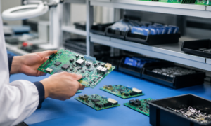
Quality Control and Testing
Quality control and testing play a crucial role in the PCBA manufacturing process. Once the components are assembled on the PCB, it is essential to ensure that everything functions correctly. Various tests are conducted to check for any defects or faults in the circuit board.
The first step in quality control is visual inspection, where trained technicians examine the board for any visible issues such as soldering defects or misplaced components. Next, automated optical inspection (AOI) machines scan the PCB for errors with precise accuracy.
After visual inspection, functional testing is performed to verify that all components work together as intended. This test ensures that the final product meets all required specifications and standards before proceeding to packaging and shipping. Quality control measures help maintain high standards of production and customer satisfaction in PCBA manufacturing processes.
Packaging and Shipping
Once the PCBA manufacturing process is complete and quality control measures have been conducted, the next crucial step is packaging and shipping. This final stage ensures that the assembled PCBs are protected during transportation to their destination.
Packaging involves carefully placing the printed circuit boards in appropriate containers or boxes to prevent any damage that could occur during transit. Special care must be taken to secure components and prevent any movement that may lead to dislodgment or breakage.
After packaging, the PCBAs are labeled accurately for identification purposes. Clear labeling helps streamline the shipping process and ensures that each package reaches its intended recipient without confusion.
Shipping plays a vital role in delivering the finished products to customers efficiently. Choosing reliable carriers with experience in handling delicate electronic components is essential for safe delivery.
Proper packaging and efficient shipping are critical steps in ensuring that PCBA products reach their destination intact and ready for use by customers.
Advancements in PCBA Manufacturing Technology
Advancements in PCBA manufacturing technology have revolutionized the way electronic devices are produced. With the introduction of automation and robotics, the assembly process has become more efficient and precise.
One notable advancement is the use of AI-driven software for PCB layout design, which helps optimize component placement for better performance. Additionally, 3D printing technology is now being utilized to create custom enclosures and components, reducing production time and cost.
Furthermore, the implementation of IoT (Internet of Things) connectivity allows manufacturers to monitor and control equipment remotely, enhancing overall productivity. Machine learning algorithms are also being employed for predictive maintenance, minimizing downtime and improving reliability.
These advancements in PCBA manufacturing technology are shaping the future of electronics production by streamlining processes and pushing boundaries in innovation.
Conclusion
The PCBA manufacturing process is a complex yet fascinating journey that involves precision, advanced technology, and meticulous attention to detail. From designing the PCB layout to testing and packaging the final product, each step plays a crucial role in ensuring high-quality electronic components for various industries.
As advancements continue to drive innovation in PCBA manufacturing technology, we can expect even more efficient processes, improved quality control measures, and faster turnaround times. The future of PCBA manufacturing looks promising as manufacturers strive to meet the growing demands of the electronics market while maintaining high standards of excellence.
Whether you’re a consumer using electronic devices on a daily basis or a company seeking reliable PCB assemblies for your products, understanding the intricate process behind PCBA production can give you a newfound appreciation for the skill and expertise involved in bringing these essential components to life.
Read More From Techbullion