The semiconductor industry has been leveraging Artificial Intelligence (AI) and Machine Learning for nearly a decade. However, Generative AI (GenAI) has been integrated into various initiatives in recent years. The users of GenAI applications, including critical internal and external stakeholders such as executive leaders, employees, third parties, and customers, play a crucial and empowering role in evaluating the GenAI technology for its benefits and potential issues, thereby shaping its future use.
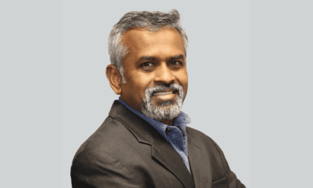
“Technology risks in the semiconductor industry are traditionally considered risks related to only IT systems and infrastructure. However, GenAI brings a set of new and complex risks dramatically changing the technology risk landscape in the semiconductor industry”, says well-respected technology risks expert Vikas Kumar.
According to Vikas Kumar, GenAI’s risks are unprecedented in semiconductor organizations and have the potential to significantly disrupt operations, impact finance, and tarnish the semiconductor industry’s reputation.
Vikas Kumar adds: “Currently, GenAI is used in every business operation of the semiconductor industry – Sales, Marketing, R&D, Finance, Pricing, IT, and Manufacturing and the use of GenAI will continue to increase in the semiconductor industry as it brings efficiency and innovation. Therefore, it is critical to understand and highlight the risks associated with GenAI. Performing an assessment or readiness check exercise will help understand the governance requirements that will mitigate risks associated with GenAI deployment, including biases, security vulnerabilities, and unintended consequences.”
Vikas Kumar says, “Addressing GenAI governance at an early adoption stage is crucial for the semiconductor industry.” He believes that by establishing a solid foundation for GenAI governance, the semiconductor industry can ensure that AI models are ethical, sustainable, transparent, and accessible.”
While working in leady Big4 technology consulting firms such as Deloitte, KPMG, and Capgemini, Vikas Kumar has helped numerous highly valued billion-dollar clients in the technology and utilities sectors to implement the GenAI governance, guidelines, and control frameworks, which enabled them to promote transparency and accountability in the development and use of AI and automation, standardize operation around GenAI, mandate minimum standards of security and risk controls, and increase trust in AI systems. Vikas Kumar has implemented GenAI related risk framework for semiconductor and robotics clients. One example of the risk initiatives related to GenAI he implemented was Role-Based Access Control (RBAC)- RBAC, which is a fundamental concept in cloud security. It allows clients to manage access to resources based on roles assigned to users or groups and controls related to bots created by GenAI for logging into the financial system and downloading reports into CSV format and e-mail to analysts in Finance as part of their weekly tasks.
GenAI a New Emerging Risk for the Future
Effective AI governance minimizes risks and safeguards the semiconductor organization’s reputation. In summary, prioritizing GenAI governance at the outset is essential when planning to embed and scale these technologies across an enterprise. It sets the stage for responsible AI adoption, mitigates risks, and fosters stakeholder trust.
About Vikas Kumar
Vikas Kumar is a distinguished technology risk professional with over 15 years of experience in device fabrication, technology auditing, and data security risk management. Beginning his career as a researcher at Massachusetts Institute of Technology, USA, while working on semiconductor device fabrication, he published several international journals and conferences on the application of semiconductor devices in renewable energy and memory devices. As he progressed in his journey, he played a critical role in all aspects of semiconductor device processing, including but not limited to device fabrication, technology risk assessment, and emerging risks such as GenAI in semiconductor operation.
Vikas Kumar has a double master’s degree in material and microsystem engineering from the University of Alberta, Canada, and Masdar Institute, in collaboration with the Massachusetts Institute of Technology, USA, focusing on process optimization and technology risks aspects of semiconductor devices.


