BGA Substrates Fabrication. Alcanta PCB has made many 2 layer to 14 layers BGA Substrates PC Board. and the drilling ways are any layers interconnection. high quality and fast shipping time.
A printed circuit board is a complex mechanism that runs an electronic device. Without it, the device simply wouldn’t work. There are so many important parts of a PCB that it can be difficult to understand how it operates. Let’s look at different parts of a PCB to understand what it is and why it’s there.
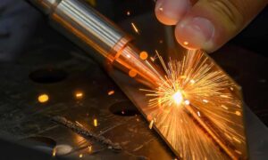
A BGA (ball grid array) is a decedent of a PGA (pin grid array), which is part of the complex maze of circuitry on a PCB. PCB manufacturers use BGA to package those integral components onto the board, or the substrate. Metal balls made from solder attach to the laminated underside of the board to hold the components together. The BGA must get soldered to secure the components to the board.
The pins go in a grid pattern on the board. They conduct electrical signals between all the integrated circuits on the PCB. The small solder balls you see on the substrate are the BGAs.
BGA is nothing but ball grid array which is a type of surface mount technology( SMT ), and it means soldering between components and PCB. BGA consists of many overlapping layers that include one to a million multiplexers, logic gates, flip-flops or other circuits. BGA is a familiar component for PCB, BGA components are packaged electronically into standardized packages that contain a variety of shapes and sizes, and it’s famous for its high lead count, tiny inductance and highly-efficient density. there is no doubt that the application of BGA plays an important role in PCB fabrication.
BGA package types
There are mainly three BGA types as following based on different substrates:
- PBGA (Plastic Ball Grid Array)
- CBGA (Ceramics Ball Grid Array)
- TBGA (Tape Ball Grid Array)
PBGA ( Plastic BGA ): a multilayer PCB that takes BT resin/glass laminate as the substrates, and plastic as the packaging material. PBGA is mainly in middle to high effective devices that meet the demands of low cost, low inductance, ease of surface mounting but high-level reliability for packaging. In addition, PBGA has some additional copper layers in the substrates as dealing with power dissipation.
TBGA (Tape BGA ): a structure with a cavity, which is a good solution for applications with heat dissipation but no external heatsink. There are two kinds of interconnections between chip and substrate: inverted solder bonding and lead bonding.
CBGA ( Ceramics BGA ): it takes multi-layer ceramic as the substrate. The metal cover PCB is soldered on the base substrate with sealed solder to protect the chip, lead and pad.
If you have any questions, please feel free to contact us with info@alcantapcb.com , we will be happy to help you.
The benefits of using BGA substrates are numerous, including increased reliability, improved thermal performance, and enhanced electrical properties. However, there are also some drawbacks to consider such as higher costs for production due to its complexity.
With the growth and advancement of technology constantly pushing towards miniaturization and increased functionality requirements from electronics devices; BGA Substrates will continue to play a crucial role in meeting these demands.