Santa Clara, CA — May 19, 2025 — When our smartphones perform seamlessly or medical devices operate with precision, we rarely consider the unseen engineering challenges that had to be overcome. In the semiconductor industry, where devices are measured in nanometers, engineers tackle problems most people never know exist.
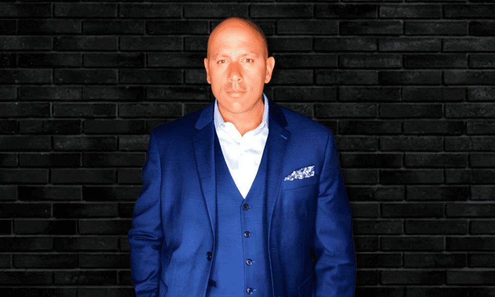
One such engineer is Akshay Harlalka, who has spent years working on solutions that most of us will benefit from without ever knowing it.
“Most of engineering is invisible to the end user, and that’s exactly how it should be,” says Harlalka, currently a Staff Mechanical Design Engineer at Atomic Machines Inc. “When we’ve done our job right, the technology just works.”
This self-effacing approach contrasts with Harlalka’s significant contributions to semiconductor manufacturing technology. During his tenure at ASML—the Dutch company that holds a leading position in advanced lithography machines required to manufacture cutting-edge microchips—he developed innovations that addressed one of the industry’s most persistent challenges: the costly downtime of machines that can amount to millions of dollars in opportunity costs. As an inventor on patents related to these solutions, Harlalka’s work has been implemented in semiconductor fabrication facilities where even minutes of unnecessary downtime translate to substantial production losses in an industry already struggling to meet global demand.
Those innovations proved valuable enough to be protected by multiple patents, including US11953838B2 and TWI792198B. Industry experts estimate that such maintenance improvements can save fabrication facilities millions in downtime costs annually—a crucial advantage in an industry where production delays impact everything from car manufacturing to smartphone availability.
“The semiconductor supply chain is incredibly interdependent,” Harlalka explains during our interview at a coffee shop near his Santa Clara office. “A single point of failure can cascade through the entire system. Our focus is always on predicting and eliminating those potential failure points as early as possible.”
Finding Real-World Applications for Theoretical Problems
When not developing machinery for semiconductor manufacturing, Harlalka turns his engineering mind to other challenges. In 2022, he published research in the ASME Open Journal of Engineering that addressed a common but complex issue in mechanical systems: understanding and predicting the stiffness of bolted connections.
Professor Alex Slocum from MIT, who co-authored the research with Harlalka, describes the work as providing “engineers with a practical tool for more efficiently predicting joint stiffness.” As the Walter M. May and A. Hazel May Chair in Emerging Technologies at MIT and a member of the National Academy of Engineering, Slocum’s assessment carries significant weight in the field.
Harlalka seems equally comfortable applying his expertise to social challenges. His research on preventing vaccine freezing in cold chains tackled the surprisingly common problem of vaccines becoming unusable due to freezing during distribution in developing regions.
“That project started with a simple observation that the existing vaccine delivery solutions were not optimal for use in underdeveloped countries where health workers are not educated on vaccine freezing risks,” he says.
“The technical principles remain consistent whether you’re designing components for semiconductor equipment or solutions for vaccine delivery,” says Harlalka. “It’s about understanding the physics, identifying the critical variables, and creating robust systems that perform reliably under variable conditions.”
Recognition Beyond Engineering
Despite his technical focus, Harlalka has found time to give back to his alma mater. A few years ago, his contributions to the MIT Alumni Angels of Northern California earned him the MIT Great Dome Award, the highest honor bestowed by the MIT Alumni Association.
“The award was unexpected,” he admits with characteristic modesty. “I’ve simply tried to help create connections between MIT’s innovation ecosystem and Silicon Valley’s entrepreneurial community.”
Professor Slocum, who has maintained a professional relationship with Harlalka since his time as a student, notes in his assessment that his former student’s “record of achievement to date more than evidences the indispensability of his work to US industry.”
Looking Forward: The Next Engineering Challenges
These days, Harlalka focuses on 3D inspection technology for MEMS devices at Atomic Machines. “These devices are in everything now—your phone, your car, medical equipment,” he explains. “The challenge is inspecting components that are not just tiny, but have complex three-dimensional structures that must function perfectly.”
As our conversation wraps up, I ask what keeps him motivated to tackle these invisible problems day after day. He pauses before answering.
“Engineering isn’t about the glory,” he says finally. “It’s about the satisfaction of knowing you’ve solved a problem that makes technology better, more reliable, or more accessible. Most people will never know about the specific problems we’ve solved, but they’ll benefit from the solutions every day.”
Akshay Harlalka earned his Master’s degree from MIT and previously worked at ASML and Applied Materials before joining Atomic Machines. His research has been published in engineering journals, and he remains active in MIT alumni activities in Northern California. For more information about his work, visit his website at https://www.akshayharlalka.com/.