Semiconductor packaging plays a crucial role in modern electronics by protecting the chip, enabling electrical connections, and managing heat dissipation. As the industry moves toward miniaturization, high-performance computing, and heterogeneous integration, packaging technologies continue to evolve. This article provides a deep dive into the fundamentals, types, processes, and future trends in semiconductor packaging.
Introduction
What is Semiconductor Packaging?
Semiconductor packaging refers to the process of enclosing and interconnecting semiconductor chips to ensure their functionality, protection, and compatibility with electronic systems. It serves as the bridge between the silicon die and the external environment, enabling power delivery, signal transmission, and heat dissipation.
The Importance of Semiconductor Packaging
The performance and reliability of semiconductor devices depend significantly on their packaging. Key factors influenced by packaging include:
- Electrical Performance: Signal integrity, power delivery efficiency, and high-speed data transmission.
- Thermal Management: Dissipating heat efficiently to prevent overheating and maintain stability.
- Reliability & Durability: Protecting the chip from environmental factors such as moisture, contaminants, and mechanical stress.
- Form Factor & Miniaturization: Enabling compact, high-density designs in applications like smartphones, wearables, and IoT devices.
Growing Demand for Advanced Packaging
As computing power increases and Moore’s Law slows down, there is a growing demand for advanced packaging techniques such as 2.5D and 3D integration. These technologies are essential for high-performance computing, AI accelerators, 5G networks, and automotive electronics.
Fundamentals of Semiconductor Packaging
Core Functions of Semiconductor Packaging
The packaging process serves three primary functions:
- Chip Protection – Encapsulation shields the silicon die from environmental damage and mechanical stress.
- Electrical Interconnection – Bonding wires, solder balls, or flip-chip bumps establish electrical pathways.
- Heat Dissipation – Heat spreaders and thermal interfaces enhance cooling efficiency.
Basic Components of a Semiconductor Package
A typical semiconductor package consists of the following components:
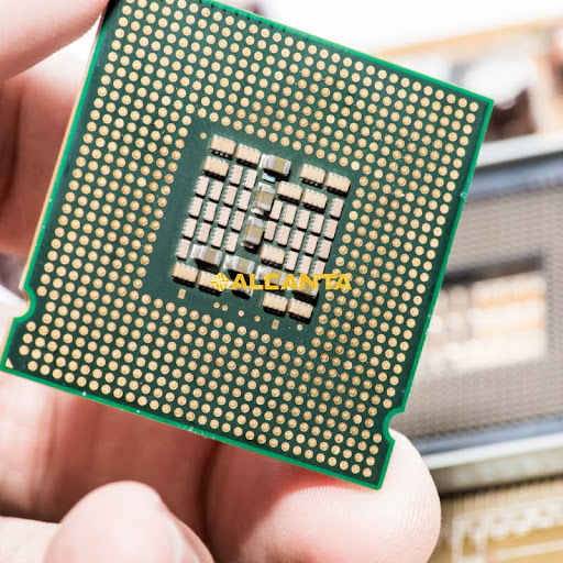
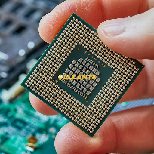
- Silicon Die – The core semiconductor chip that performs computing or signal processing.
- Substrate or Lead Frame – A mechanical and electrical support structure that connects the die to external circuits.
- Encapsulation Material – Epoxy resin, ceramic, or other materials used to protect the die from contamination.
- Interconnects – Wire bonds, solder balls, or microbumps that enable electrical connections between the die and external systems.
Interconnection Technologies
- Wire Bonding – The most common interconnect method, using fine wires to connect the die to the substrate.
- Flip-Chip – A method where the die is flipped and directly mounted onto the substrate using solder bumps.
- Wafer-Level Packaging (WLP) – Advanced technology that enables packaging at the wafer level, reducing form factor and enhancing performance.
Common Semiconductor Packaging Types
Traditional Packaging Technologies
- DIP (Dual In-line Package) – One of the earliest package types, featuring two parallel rows of pins for PCB mounting.
- SOP (Small Outline Package) – A smaller, surface-mount alternative to DIP, commonly used in consumer electronics.
- QFP (Quad Flat Package) – A package with leads extending from all four sides, often used in microcontrollers and processors.
Advanced Packaging Technologies
- BGA (Ball Grid Array) – Uses an array of solder balls for enhanced electrical and thermal performance, commonly used in CPUs and GPUs.
- CSP (Chip Scale Package) – A package nearly the same size as the die, enabling miniaturization in mobile devices.
- WLP (Wafer-Level Packaging) – An advanced packaging method where the entire wafer is packaged before dicing, reducing cost and improving performance.
3D Packaging and Emerging Technologies
- TSV (Through-Silicon Via) Packaging – Uses vertical interconnects through silicon wafers to achieve high-speed, high-density integration.
- Fan-Out Packaging – An advanced technique that redistributes I/O connections beyond the chip’s original footprint, improving electrical performance.
- 3D IC (Stacked Integrated Circuit) – Stacks multiple chips on top of each other, reducing power consumption and improving bandwidth.
Key Semiconductor Packaging Processes
Front-End Packaging Processes
- Wafer Dicing – Cutting the processed wafer into individual dies.
- Die Attach & Interconnection – Bonding the die to the substrate using wire bonding, flip-chip, or other methods.
- Encapsulation – Using epoxy resin or ceramic to protect the die.
Back-End Packaging Processes
- Electrical Testing – Functional and reliability tests to ensure performance.
- Package Assembly – Solder ball attachment, heat spreader integration, and PCB mounting.
- Packaging Optimization – Signal integrity tuning, heat dissipation enhancements, and design miniaturization.
Impact of Packaging on Semiconductor Performance
Electrical Performance
- Signal propagation speed, power integrity, and electromagnetic interference (EMI) considerations.
Thermal Management
- Techniques such as heat sinks, thermal vias, and phase-change materials to manage heat dissipation.
Reliability & Mechanical Strength
- Ensuring the package withstands mechanical shocks, vibrations, and extreme temperature variations.
Miniaturization & High-Density Integration
- The role of fan-out, 3D stacking, and WLP in enabling smaller, more powerful devices.
Emerging Trends in Semiconductor Packaging
Chiplet and Advanced Packaging
- Chiplet Architecture – Breaking down monolithic chips into modular chiplets for performance and yield improvements.
- 2.5D & 3D IC – Leveraging interposers and stacking techniques to enhance bandwidth and reduce power consumption.
Material Innovations
- High-Thermal Conductivity Materials – Graphene, diamond, and advanced ceramics for heat dissipation.
- Low-Loss Dielectrics – Essential for high-frequency applications like 5G and radar systems.
Heterogeneous Integration
- Multi-Chip Packaging – Combining processors, memory, and specialized accelerators in a single package.
- MEMS & Photonics Integration – Integrating optical and MEMS devices with traditional silicon electronics.
Automation & AI in Packaging
- AI-Driven Design Optimization – Machine learning techniques for improving layout, material selection, and thermal performance.
- Smart Manufacturing – Using robotics and advanced sensors to automate packaging processes.
Conclusion & Future Outlook
Semiconductor packaging is becoming increasingly critical as device complexity grows and Moore’s Law slows down. Innovations in materials, interconnects, and 3D integration are driving new possibilities for high-performance computing, AI, and telecommunications. While challenges such as cost, thermal management, and reliability remain, ongoing advancements in packaging technology will continue to shape the future of the semiconductor industry.