
Over the next 10 years, the global market for 3D through-silicon-via (TSV) devices is anticipated to grow at a CAGR of 20%, according to Fact.MR is a supplier of market research and competitive intelligence.
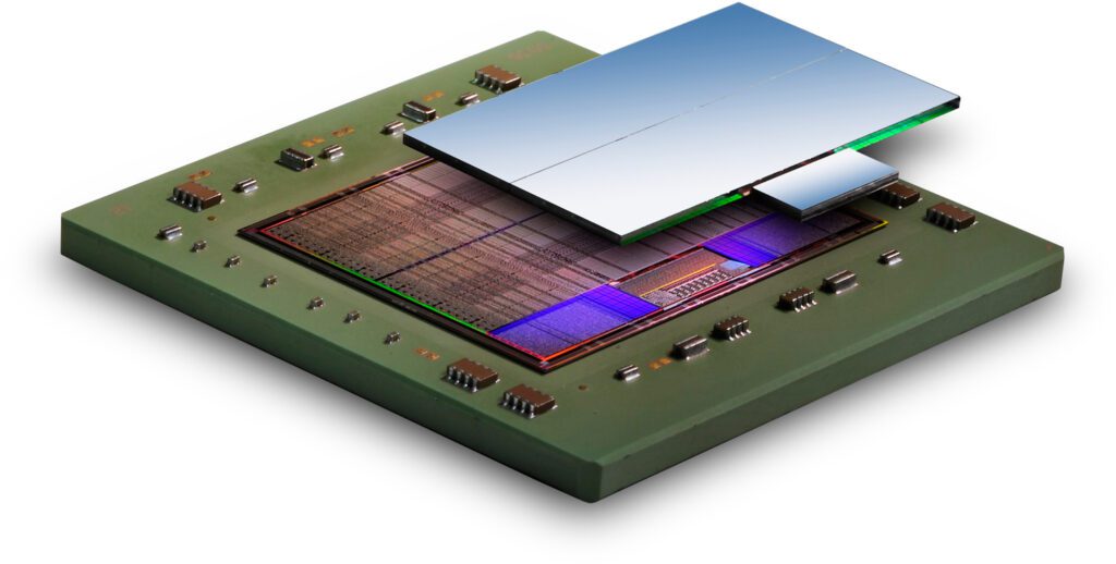
As a highly sophisticated semiconductor packaging approach that significantly enhances chip performance and functionality, 3D through-silicon-via technology is quickly gaining popularity. Semiconductor manufacturers are employing TSV techniques for chip stacking more and more to reduce package space requirements, especially for next-generation devices, and to satisfy edge computing application needs for faster response times and diverse architectures.
3D through-silicon-via technology has advanced quickly within the global semiconductor industry, driven by growing demand from international electronics manufacturers for cutting-edge, high-performance chip architectures and designs in advanced packaging with superior performance, power consumption, and form factor features.
Industries are embracing 3D TSV devices for production processes because of factors like the spread of cloud-based apps, a strong information and communication technology perspective, and continued advancements in DRAM and intelligent lighting.
With prospects in consumer electronics, information and communication technology, automotive, military, aerospace, and defense industries, the market for 3D through-silicon-via devices has a bright future.
Key Market Study Conclusions
- The market for 3D through-silicon-via devices will reach US$ 15 billion by 2031.
- By 2031, 3D TSV memory sales are anticipated to exceed $5 billion.
- Over the next ten years, CMOS image sensors are expected to see CAGRs of over 18%.
- Market share in the Asia Pacific region exceeds 50%.
- By 2031, the Japanese market is anticipated to be worth $3 billion.
- Market growth in South Korea is anticipated to be 16% between 2021 and 2031.
Marketplace rivalry
The growth of their commercial operations in developing regions is a key emphasis for numerous well-known manufacturers in the market for 3D TSV devices.
- For its cutting-edge system-on-integrated chips (TSMC-SoIC), TSMC unveiled ANSYS (ANSS) solutions for sophisticated 3D chip stacking technology in April 2019. This was done to provide customers with increased performance and power efficiency for extremely complex and demanding cloud and data center applications.